
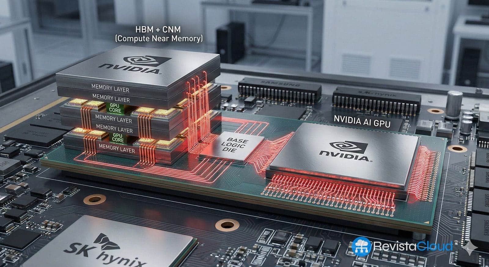
NVIDIA has reportedly asked Samsung, SK hynix and Micron to manufacture the base die of its custom HBM memory, called NVHBM, using TSMC’s 3-nanometer process, according to South Korean outlet Seoul Economic Daily, picked up by Wccftech. The goal would be to unify production across the three suppliers to cut down on validation steps. None of the companies has confirmed this.
NVIDIA’s custom HBM in 20 seconds
- According to the Korean press, NVIDIA wants NVHBM’s base die built on TSMC’s 3nm node.
- Samsung, which builds its base dies in-house, is said to have agreed.
- NVIDIA announced NVHBM on August 26 and claims up to 30% more bandwidth than HBM4E.
- No sample or production dates have been given.
The base die is the logic chip that sits underneath the stacked DRAM layers in each HBM module and manages communication with the processor. Early generations were built using memory manufacturing processes, but since HBM4 it’s made with faster, more efficient logic foundry processes. Each memory maker has handled that part its own way, and that’s reportedly where NVIDIA wants to bring order.
What NVHBM Is and What NVIDIA Has Announced
What is official is the underlying technology. NVIDIA introduced NVHBM on August 26 as part of the expansion of its NVLink Fusion program, which lets third-party accelerators connect to its rack-scale platform. The idea is to move the memory controller — until now built into the accelerator chip — onto the HBM’s base die, replacing the wide parallel bus of the JEDEC standard with a narrower, NVIDIA-designed serial link. We covered this when explaining how NVIDIA moves the memory controller into HBM.
According to company figures reported by TechRadar, NVHBM would deliver up to 30% more bandwidth per stack, up to 15% lower power consumption, and up to 25% more usable area on the accelerator chip, always compared against standard HBM4E samples. Counterpoint Research notes that the only figure that’s easily verifiable is the 67% reduction in interface area, since reference HBM4E isn’t shipping in volume yet.
The timeline isn’t clear either. SamMobile pointed in August to a debut with Rubin Ultra next year, while NVIDIA confirmed in March, at its GTC conference, that Feynman, the generation planned for 2028, will carry custom HBM, as we reported when covering NVIDIA’s plans for Feynman. The Korean report gives no sample or production dates.
Why This Mainly Affects Samsung
SK hynix and Micron already rely on outside foundries, chiefly TSMC, for their advanced base dies, so the request fits what they already do. Samsung is the exception: it designs and manufactures the base die on its own lines, using its 4nm process for HBM4, and has stuck to that integrated model. According to Seoul Economic Daily, the Korean company has agreed to make NVHBM’s base die at TSMC, though it would still build its standard HBM in-house and is weighing using its own foundry if demand outstrips TSMC’s capacity.
The move isn’t entirely new. In mid-September, Korean outlet iNews24 had already reported that Samsung was keeping the option open to use TSMC for the base die of its custom HBM if a customer asked for it, with no contract confirmed. It also fits SK hynix’s strategy, which is validating HBM5 with TSMC. For NVIDIA, the advantage would be having a single design and a single process to validate, instead of three different variants.
The less visible side is the power NVIDIA gains over the supply chain. If it designs the base die and decides where it’s made, memory makers end up producing to its specification, and TSMC adds another piece of the HBM module. Wccftech links the HBM boom to analysts’ forecasts that losses at Samsung’s foundry division will fall from 6.74 trillion won in 2025 to 3.92 trillion won in 2026 — an estimate that doesn’t come from the company itself.
FAQ
What is NVHBM?
It’s the custom HBM memory NVIDIA unveiled on August 26. It moves the memory controller onto the module’s base die and uses an NVIDIA-designed serial link instead of the JEDEC standard bus.
Is it confirmed that Samsung will manufacture at TSMC?
No. It’s reported by the Korean press based on industry sources, and neither NVIDIA, Samsung nor TSMC has confirmed it.
When will NVIDIA’s custom HBM arrive?
There’s no official date. Some outlets mention Rubin Ultra in 2027, and NVIDIA has confirmed custom HBM for Feynman, planned for 2028.
Sources:
- Wccftech: NVIDIA’s custom HBM, Samsung and TSMC’s 3nm base die
- TechRadar: Nvidia unveils custom high bandwidth memory
- Counterpoint Research: The trillion dollar bottleneck, NVIDIA’s NVHBM fight for base die
- SamMobile: Samsung could supply NVHBM chips to NVIDIA
- iNews24: Is Samsung also teaming up with TSMC? Custom HBM blurs the lines in semiconductors
