
SK hynix has jointly validated next-generation HBM5 memory with TSMC using CoWoS packaging technology, work that puts both companies in an early stage of preparation for future artificial intelligence accelerators. The collaboration was unveiled during TSMC’s Open Innovation Platform (OIP) conference held on September 23 in Santa Clara, where SK hynix also showed its HBM4 integrated into NVIDIA’s Vera Rubin superchip.
HBM5 and TSMC’s key facts in 20 seconds
- SK hynix and TSMC have validated HBM5 on CoWoS for future AI systems.
- SK hynix’s HBM4 already appears integrated into NVIDIA’s Vera Rubin superchip.
- The company showed 48 GB HBM4E, 48 GB HBM4, and 36 GB HBM3E.
- SK hynix received TSMC’s Partner of the Year award for the second year running.
- The alliance is also advancing on SSDs, PCIe, chiplets, and new AI memory solutions.
Collaboration between memory makers and foundries is gaining weight as AI accelerators pack in ever-larger amounts of high-bandwidth memory. TSMC uses its OIP platform to bring together memory, design, IP, packaging, and manufacturing companies, with the goal of validating technologies before they reach commercial products.
For SK hynix, the relationship with TSMC already spans several generations of HBM and packaging technologies. The new step consists of validating HBM5 on CoWoS, TSMC’s 2.5D packaging technology used to place processors and HBM memory inside the same high-performance package.
HBM5 gets tested ahead of the next wave of accelerators
The reference to HBM5 is one of the most notable elements of SK hynix’s presentation. The company says its packaging development organization and TSMC worked together from the earliest stages to check this memory’s integration with CoWoS.
The validation doesn’t amount to an announcement of mass HBM5 production, nor does it point to a specific commercial product that will use it. What it shows is that the integration between memory and packaging is already being prepared ahead of the systems that will need this generation of HBM.
The technical reason ties back to how memory itself is evolving. As the number of stacked layers and the bandwidth increase, memory stops being a component that can be developed entirely independently of the processor and the packaging. The package has to provide enough connections to take advantage of HBM’s specs while keeping signals and power within the system’s requirements.
TSMC keeps CoWoS as one of its main technologies for high-performance computing systems. Its platform allows different chips and HBM modules to be integrated on an interposer, and the company keeps expanding interposer size to accommodate more logic and memory.
SK hynix is already part of TSMC’s 3DFabric alliance alongside other memory makers such as Micron and Samsung. That structure is specifically aimed at making it easier to integrate memory, logic, and packaging technologies for next-generation systems.
HBM4 is already riding along with Vera Rubin
While HBM5 remains in the validation stage, SK hynix showed off a much more immediate application of its technology at its booth: NVIDIA’s Vera Rubin superchip fitted with the company’s HBM4 memory.
The configuration on display included 12-layer, 36 GB HBM4, along with a 96 GB SOCAMM2 module. SK hynix explained that HBM4 sits around Rubin’s GPU core to provide a high-bandwidth data channel, while SOCAMM2 acts as main memory for the Vera CPU.
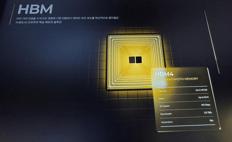
The company also brought other products from its lineup to the conference. These included a 12-layer, 48 GB HBM4E, a 16-layer, 48 GB HBM4, and a 12-layer, 36 GB HBM3E. The comparison shows how memory capacity grows as generations and stacking configurations evolve.
HBM, or high-bandwidth memory, uses multiple DRAM chips stacked vertically to deliver high data-transfer capacity in a compact footprint. In AI accelerators, its job is to keep a fast flow of data between memory and the processors carrying out compute-intensive operations.
Physical integration carries more and more weight. Rising HBM capacity and bandwidth need to be matched by packaging systems capable of connecting more memory with more logic. That’s why SK hynix is working with TSMC before HBM5 reaches product stage.
SK hynix’s memory strategy goes beyond HBM
SK hynix’s showcase wasn’t limited to high-bandwidth memory. The company also presented new generations of server DRAM and SSDs aimed at data centers.
Among the products on display were a 256 GB 3DS RDIMM, a 128 GB MRDIMM module, and a 64 GB RDIMM based on its 10-nanometer-class 1c process. It also showed E1.S, E3.S, and M.2 SSDs for different server environments.
In storage, SK hynix is also preparing chiplet-based SSD controllers for future PCIe generations. According to the company, these designs split conventional controller functions across several chiplets connected via UCIe, an open standard for chip-to-chip communication within the same package.
The company frames this evolution within the growth of AI infrastructure. During a joint presentation with Cadence, Daesik Park, an SK hynix distinguished engineer specializing in PCIe, said the PCIe-based enterprise SSD market could grow from 509 exabytes in 2026 to 1,933 exabytes in 2030. That’s a forecast presented by SK hynix, not an independent market figure.
The company is also developing a technology called HBF, or High Bandwidth Flash, conceived as a possible memory layer sitting between HBM and SSD. SK hynix describes it as a NAND-based solution that aims to combine capacity greater than HBM’s with high bandwidth and a different cost per capacity.
The conference’s message, then, is broader than the launch of a new memory type. SK hynix is preparing different layers of storage and memory for AI systems, while TSMC develops the packaging technologies needed to integrate them with increasingly larger processors.
The recognition SK hynix received in Santa Clara reflects exactly that collaboration. The company won TSMC’s Partner of the Year award for the second year running, this time in the 3DFabric-HBM Integration category for its HBM5-on-CoWoS validation work.
SK hynix had already explained in June that its relationship with TSMC was expanding toward future HBM generations and advanced packaging, while also looking for opportunities in custom memory for large tech customers.
HBM4 represents the generation now being integrated into next-generation AI systems, while HBM5 still belongs to a development and validation stage. The gap between the two technologies shows how memory is being designed increasingly earlier alongside the processor and the packaging. In systems where compute capacity is growing fast, the connection between these elements determines how much of that performance can actually be put to use.
Frequently asked questions
What has SK hynix validated with TSMC?
SK hynix and TSMC have validated HBM5 using TSMC’s CoWoS packaging technology to prepare for next-generation AI systems. The company has not announced immediate mass production of HBM5 with this step.
Which HBM does NVIDIA’s Vera Rubin superchip use?
SK hynix showed Vera Rubin with 12-layer, 36 GB HBM4, plus a 96 GB SOCAMM2 module. The company also displayed other HBM4 and HBM4E configurations.
What is CoWoS?
CoWoS, short for Chip on Wafer on Substrate, is a TSMC packaging technology that integrates chips such as processors and HBM inside the same package via an interposer. TSMC uses it for high-performance computing applications.
What other memory is SK hynix preparing for AI?
The company showed server DRAM, enterprise SSDs, and chiplet-based solutions for future PCIe generations. It also presented HBF as a possible new memory layer between HBM and SSD.
via: news.skhynix
