
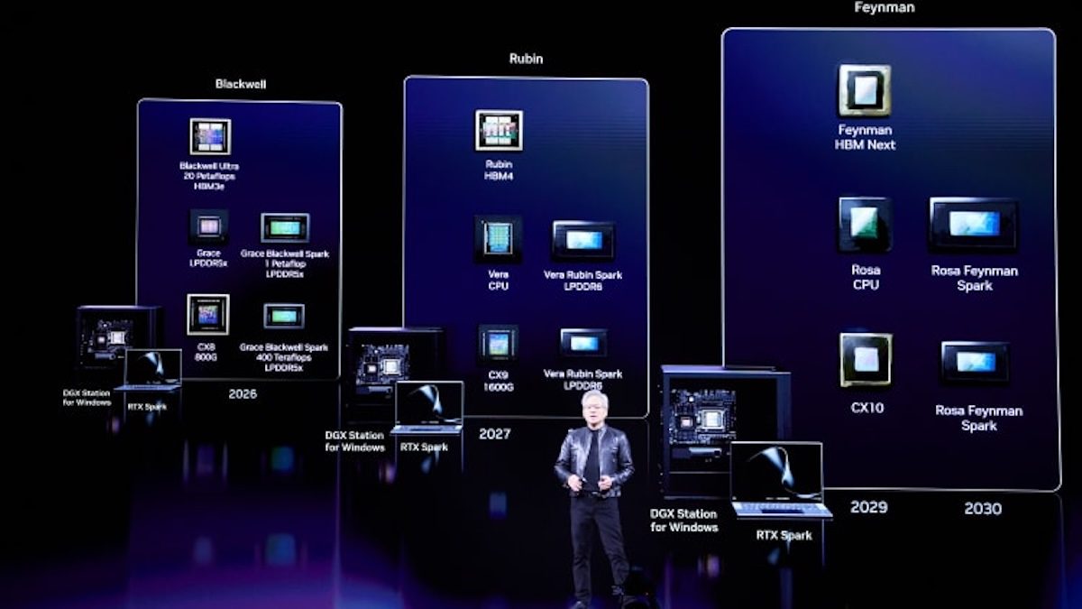
NVIDIA is still bringing Vera Rubin to market, but its next major AI platform is already starting to take shape. Feynman is officially scheduled for 2028, while new information from the Taiwanese supply chain points to a particularly ambitious combination: TSMC A16 process, 3D integration with SoIC, custom HBM memory, and optical connections via CPO. Some of these details have not yet been confirmed by NVIDIA and should be considered supply chain information.
The key points of NVIDIA Feynman in 20 seconds
- NVIDIA officially targets Feynman in 2028, as the successor to Vera Rubin and Rubin Ultra.
- DigiTimes points to using the TSMC A16 process, stacked chiplets via SoIC, and custom HBM.
- The platform would deepen optical connections with CPO to scale large AI systems.
- TSMC is expanding advanced packaging capacity to meet growing demand.
- Feynman exemplifies how competition is shifting from comparing GPUs to designing complete systems.
This is significant because Feynman doesn’t seem to be just a GPU with more transistors. The evolution of large AI accelerators is forcing solutions to four simultaneous problems: manufacturing denser chips, powering those chips, bringing memory and computation closer together, and moving increasing amounts of data between accelerators.
Here is where technologies once analyzed separately begin to converge within a single platform.
TSMC A16 and SoIC: the leap isn’t only inside the GPU
According to DigiTimes, NVIDIA is shifting development and supply chain resources toward Feynman with production planned for the second half of 2028. The Taiwanese publication indicates that the platform would use A16, one of TSMC’s most advanced high-performance computing technologies.
It’s important to distinguish confirmed information from leaks here.
TSMC has publicly detailed the features of A16. This technology combines nanosheet transistors with Super Power Rail (SPR), its late-stage power delivery system. By relocating some power distribution to the backside, more interconnect resources are available on the front for signals.
Compared to N2P, TSMC promises that A16 will deliver 8-10% higher speed at the same voltage, or 15-20% lower power consumption at equal performance, plus up to 1.10 times the chip density. It is expected to be available for production in the second half of 2026.
However, the use of A16 in Feynman currently comes from supply chain sources, not an official NVIDIA specification.
A similar situation applies to packaging.
Taiwanese reports suggest Feynman will increase use of SoIC (System on Integrated Chips), TSMC’s 3D integration technology. Instead of just placing components side by side, SoIC enables vertical stacking of dies via very short interconnections.
Potential benefits are significant: reduced data movement distance, higher integration density, and lower energy consumption for certain communications between processor blocks.
This doesn’t mean SoIC will replace CoWoS. Both technologies can serve different levels within the same system. SoIC allows vertical integration of specific blocks, while solutions like CoWoS and later CoPoS can integrate large logic components and HBM memory within larger structures.
The result is that simply talking about the “manufacturing node” of a future GPU increasingly explains less about how it’s actually built.
Feynman could push rack bandwidth beyond 1 PB/s
Another critical aspect is interconnection.
For years, advancements in new accelerator generations were mainly explained by FLOPS, memory, and power consumption. Today, a growing key figure in large AI systems is: how much data accelerators can exchange and at what energy cost.
This becomes more challenging as systems grow larger.
When dozens, hundreds, or thousands of GPUs work on the same workload, increasing performance increasingly depends on the network connecting them. Copper electrical interconnects remain useful for short distances, but their consumption, signal loss, and complexity grow with higher speeds and longer distances.
That’s why NVIDIA is gradually adopting photonic technologies and Co-Packaged Optics (CPO).
DigiTimes reports that, based on the evolution of NVLink, Blackwell NVL72 can provide around 130 TB/s of total bandwidth per rack. Vera Rubin could increase this to about 260 TB/s, and Rubin Ultra to roughly 520 TB/s.
For Feynman, supply chain forecasts estimate system bandwidth exceeding 1,040 TB/s, breaking the 1 PB/s barrier per rack for the first time. DigiTimes also mentions Feynman NVL72, NVL144, and an NVL1152 configuration made up of eight Kyber racks. These are roadmap estimates and not final product specs, so they may still change.
Optics will be essential technology to sustain such scale.
TSMC has been developing its photonics technology COUPE (Compact Universal Photonic Engine). Its approach uses SoIC to integrate electronic and photonic circuits, bringing the conversion between electrical and optical signals closer to the chip’s package.
Feynman could become one of the earliest major examples of how computing, advanced packaging, and photonics no longer evolve as separate components.
Custom HBM and immense packaging pressures
Memory forms the third element.
DigiTimes mentions custom HBM for Feynman, though official specs regarding capacity, bandwidth, stacks, or specific features are not yet available.
It’s advisable to avoid designations like HBM4E or HBM5 for now.
The key point is that high-bandwidth memory is no longer just a component placed around a GPU. The design of the accelerator, memory interface, packaging, and HBM characteristics are increasingly interconnected.
This evolution is also pressuring TSMC.
DigiTimes reports that TSMC is accelerating its AP7 (Chiayi) and AP8 (Tainan) facilities to boost advanced packaging capacity. Demand is no longer only coming from CoWoS: SoIC, CoWoS-L, future CoPoS solutions, and CPO-related technologies must grow simultaneously.
Additionally, TSMC has reportedly revised its SoIC plans to meet customer demands from NVIDIA and AMD, aiming for about 50,000 wafers per month by late 2027. These figures are from the supply chain sources and are not final commitments from TSMC.
This highlights an often less visible aspect in the AI race: designing a faster GPU is insufficient if there isn’t enough packaging, memory, substrates, optical components, or electrical capacity to support it.
Feynman confirms the race is now at rack scale
NVIDIA outlined a roadmap during GTC 2026 where Feynman appears after Vera Rubin and Rubin Ultra. However, new data from Taiwan suggest even broader possibilities.
If A16, SoIC, custom HBM, and CPO all come together in the 2028 platform, Feynman will be much more than just NVIDIA’s next GPU.
It will also test the entire supply chain.
TSMC will need to produce silicon and have sufficient advanced packaging capacity. Memory vendors must support the growth of HBM. The photonics industry will need to manufacture optical links at a much larger scale. Data center operators will have to power and cool more densely packed systems.
Furthermore, not all technology will necessarily come from TSMC. Other DigiTimes reports hint at potential limited collaboration between NVIDIA and Intel Foundry for certain 2028 components, though this information isn’t officially confirmed either.
Hence, the competition among NVIDIA, AMD, and Intel in 2028 likely won’t boil down to who has the fastest GPU.
The focus is shifting toward who can deliver the full system: processors, memory, packaging, switches, interconnects, optics, software, and the capacity to produce everything at volume.
Feynman is still about two years away, and many specifications could change before market release. However, the technological direction is clearer: when moving data consumes too much time and energy, simply shrinking transistors is no longer enough. It’s also necessary to rethink how the silicon is connected.
Frequently Asked Questions
When will NVIDIA Feynman arrive?
NVIDIA targets 2028 for Feynman. Supply chain sources specifically suggest the second half of that year, but NVIDIA has not announced an official commercial date yet.
Will NVIDIA Feynman use TSMC A16?
DigiTimes reports that Feynman will use A16, but NVIDIA has not officially confirmed the manufacturing node. TSMC has A16 scheduled for production starting in the second half of 2026.
What is CPO and why will it be important for AI GPUs?
CPO (Co-Packaged Optics) brings optical connections closer to the chip or switch package. Its goal is to provide high bandwidth with lower power consumption and fewer losses than certain electrical connections when AI systems reach very large scales.
What are the differences between Rubin and Feynman?
Rubin already makes extensive use of chiplets and HBM, while known information about Feynman points to greater 3D integration via SoIC, custom HBM, and more advanced optical interconnections. Final specifications have not yet been announced.
via: digitimes
