
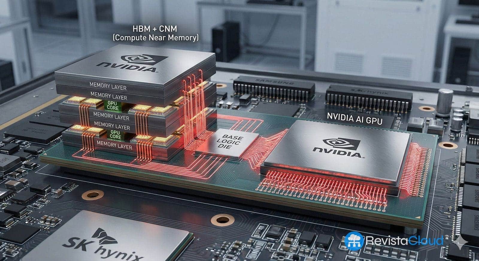
NVIDIA has unveiled NVHBM, a new high-bandwidth memory architecture that moves its memory controller off the accelerator and onto the HBM stack’s own base die. The company says the change can deliver up to 30% more bandwidth, cut HBM power consumption by 15%, and free up to 25% of the XPU’s die area compared with a conventional HBM4E implementation. The technology will be built into NVLink Fusion, and Amazon Web Services (AWS), through Annapurna Labs, is the first announced partner working with it.
NVIDIA NVHBM in 20 seconds
- NVHBM integrates NVIDIA’s memory controller directly into the HBM stack’s base die.
- NVIDIA says it delivers up to 30% more bandwidth while using 15% less power.
- The change can free up to 25% of the XPU’s die area compared with conventional HBM4E.
- Multiple memory makers will be able to supply NVHBM under a common implementation.
- Annapurna Labs will work with NVIDIA on NVHBM and NVLink Fusion for future AWS infrastructure.
The announcement lands at a time when memory has become one of the biggest factors shaping AI accelerator performance. Models with hundreds of billions or trillions of parameters need to move enormous amounts of data between memory and compute units, so adding more FLOPS does little good when the processor is stuck waiting for the data it needs.
NVHBM is specifically aimed at that relationship between compute and memory.
The controller leaves the XPU and moves into the HBM stack
In a traditional HBM architecture, the controller that manages communication with memory sits inside the accelerator itself. That means part of the silicon available on the XPU has to be set aside for memory-related functions instead of compute units.
NVIDIA is proposing to relocate that component.
NVHBM integrates NVIDIA’s custom controller inside the base die of the three-dimensional HBM stack, removing it from the XPU’s main die.
According to figures published by the company, the comparison against a standard HBM4E implementation looks like this:
| Feature | Conventional HBM4E | NVIDIA NVHBM |
|---|---|---|
| Memory controller | On the XPU | On the HBM base die |
| Bandwidth | Baseline | Up to +30% |
| HBM power consumption | Baseline | Up to -15% |
| XPU area used by controller | Built into the chip | Moved to HBM |
| Extra area available on XPU | — | Up to +25% |
| Approach | Conventional integration | Semi-custom infrastructure |
These are figures NVIDIA has published, and they’ll need to be tested against real products once NVHBM reaches commercial systems. The comparison also doesn’t mean every accelerator will automatically get 25% more performance: NVIDIA is talking about freed-up silicon area, not an equivalent amount of extra compute performance.
The advantage for chip designers lies precisely in deciding what to do with that space.
A manufacturer could use it for more compute units, bigger caches, specialized accelerator blocks, or simply a more efficient XPU design.
NVIDIA also wants a foothold in its customers’ custom chips
NVHBM matters even more when you look at it as part of NVLink Fusion, NVIDIA’s push to bring pieces of its technology into processors it didn’t design itself.
Major cloud providers have spent years developing their own accelerators to cut costs and tailor hardware to their workloads. Google has TPUs, AWS is developing Trainium and Inferentia, Microsoft has Maia, and Meta is also working on its own MTIA accelerators.
That trend could be read as a threat to NVIDIA: every custom accelerator a hyperscaler deploys is a workload that no longer has to run on its GPUs.
NVLink Fusion offers a different path.
Instead of forcing customers to choose between an NVIDIA accelerator or their own ASIC, the company wants those custom processors to be able to use pieces of its architecture, including NVLink, NVLink-C2C, NVLink Switch, MGX, and now NVHBM.
The result is an NVIDIA that tries to participate economically in AI infrastructure even when the main processor doesn’t carry its logo.
The company describes this strategy as a “vertically integrated, horizontally open” architecture. The nuance matters: the openness consists of letting third-party processors into its infrastructure, but through technologies NVIDIA itself develops.
AWS will be NVHBM’s first partner
The first announced example is particularly significant.
Annapurna Labs, Amazon’s division behind much of AWS’s custom silicon, will work with NVIDIA on NVHBM and on rack-scale NVLink architecture.
The collaboration expands on their earlier agreement around NVLink Fusion. AWS plans to bring the technology to future generations of its Trainium accelerators, starting with Trainium4.
The goal is to let Amazon’s chips and NVIDIA’s GPUs sit within a shared rack-scale architecture.
That’s a different picture from a few years ago. AWS competes with NVIDIA by developing its own accelerators, but it can simultaneously use NVIDIA’s interconnect and memory technology to build heterogeneous systems.
The resulting infrastructure can mix different types of processors depending on each workload’s characteristics.
The AI battle is shifting toward memory
The announcement also shows how accelerator design is changing.
During the early phases of the AI boom, most comparisons focused on TFLOPS or PFLOPS. As models keep growing, memory capacity and bandwidth have become just as important.
HBM stacks several layers of DRAM vertically and connects them through extremely wide interfaces. The industry has moved progressively through HBM2, HBM2E, HBM3, and HBM3E, while HBM4 and later generations push integration even further.
Moving the controller into the base die is another step in that direction: memory stops being just a component wired to the accelerator and starts taking on functions that used to belong to the processor.
NVIDIA also intends to establish a common NVHBM implementation available through multiple memory vendors.
For ASIC designers, that could cut down the work needed to integrate and validate different memories. It also lets NVIDIA extend its architecture into another strategic piece of the supply chain without necessarily becoming a DRAM manufacturer itself.
From CUDA and GPUs to controlling rack architecture
NVHBM also fits with NVIDIA’s recent business trajectory.
The company just reported that Data Center now accounts for roughly 92.5% of its quarterly revenue. In that market, it’s no longer trying to sell accelerators alone.
Its offering spans GPUs, CPUs, networking, NVLink, rack-scale systems, software, and full architectures for AI data centers. NVLink Fusion extends that strategy into the custom-accelerator market.
| Infrastructure layer | NVIDIA technologies |
|---|---|
| Compute | GPUs, Grace, and rack-scale platforms |
| Memory | NVHBM and controllers |
| Scale-up | NVLink and NVLink Switch |
| Chip-to-chip | NVLink-C2C |
| Networking | Spectrum-X and InfiniBand |
| Systems | MGX and NVIDIA racks |
| Software | CUDA and AI libraries |
| Custom chips | NVLink Fusion |
The distinction matters. NVIDIA no longer needs to manufacture every processor in a system to get its technology inside that system.
A hyperscaler can design its own XPU and still use NVLink to connect it, NVHBM for its memory subsystem, and NVIDIA technologies to integrate it into a rack-scale infrastructure.
It’s a way of adapting to the growth of custom silicon without necessarily competing head-on against it in every workload.
The open question will be how much of that extra 30% bandwidth and 15% power savings holds up once NVHBM reaches commercial products, and which memory makers sign on to the standard.
But the move is a good indicator of where AI infrastructure is heading. The competition is no longer just about building the fastest GPU. Increasingly, what matters is who controls the communication between compute, memory, and hundreds of accelerators inside the same system.
Frequently Asked Questions
What is NVIDIA NVHBM?
NVHBM is a high-bandwidth memory technology that integrates NVIDIA’s custom controller directly into the HBM stack’s base die, instead of keeping it inside the XPU.
What advantages does NVHBM promise over HBM4E?
NVIDIA says it can deliver up to 30% more bandwidth, cut HBM power consumption by 15%, and free up to 25% of XPU die area compared with a conventional HBM4E architecture.
Will NVHBM be exclusive to NVIDIA GPUs?
The announcement is specifically aimed at NVLink Fusion and third-party custom processors. NVIDIA also says it will establish a common implementation that multiple memory vendors will be able to offer.
How does AWS relate to NVHBM?
Annapurna Labs is the first announced partner working with NVIDIA on NVHBM. The collaboration is part of a broader relationship built around NVLink Fusion and future generations of AWS’s Trainium accelerators.
