
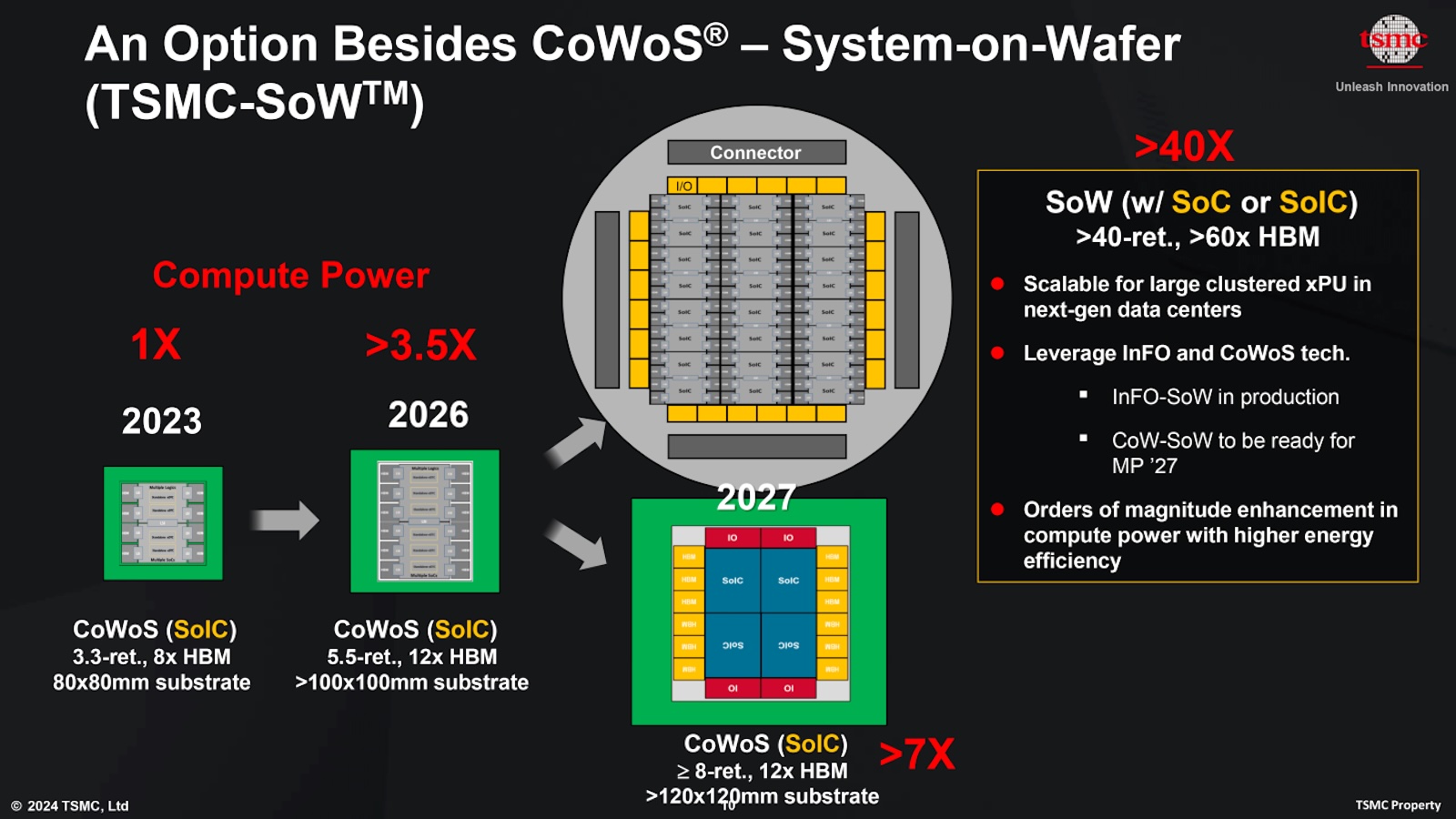
AI chips are growing so much in size and complexity that packaging has become another one of the industry’s limits. TrendForce notes that TSMC is pushing its CoWoS technology toward designs able to integrate more chips and HBM memory, while Intel is advancing EMIB-T to compete for a share of the large accelerators and ASICs used in data centers. The firm expects CoWoS-L to remain the leading advanced packaging technology for AI through 2028.
AI chip packaging in 30 seconds
- AI accelerators need increasing numbers of chips and HBM memory inside the same package.
- CoWoS-S is starting to approach its limits as designs keep growing.
- TSMC is betting on CoWoS-L, which increases effective package size using silicon bridges.
- Intel is developing EMIB-T as an alternative, with Google and AWS among the potential users.
- TrendForce expects CoWoS-L to keep leading advanced AI packaging through 2028.
The problem is tied to a part of the manufacturing process that usually gets less attention than transistor node sizes. A modern AI chip isn’t just the silicon holding its compute units. To hit the performance it needs, it also has to integrate HBM memory, other chiplets, and very high-speed connections inside a single module.
The more components that get added, the larger the package that has to be manufactured. That’s where the physical reticle limit comes in — the maximum surface area that can be exposed at certain stages of manufacturing.
CoWoS-L takes TSMC beyond conventional packaging
For the past several years, TSMC has used CoWoS-S as one of its main technologies for pairing AI processors with HBM memory. This solution uses a silicon interposer that connects the compute chips and memory modules.
According to TrendForce, CoWoS-S can currently integrate up to two SoCs or chiplets and eight HBM modules in certain configurations. That’s enough for smaller designs, but it’s starting to fall short as accelerators need more memory and more connected chips.
TSMC’s answer is CoWoS-L.
This variant builds high-speed silicon bridges into the interposer and allows for a larger effective package size. TrendForce’s chart shows a sharp progression: the reticle size associated with TSMC’s solutions goes from 3.3x in 2024 to 5.5x in 2026, 9.5x in 2027, and 14x in 2028.
The number of components that can be integrated also grows. In TrendForce’s forecast, the number of SoCs or chiplets goes from two to four in 2026, eight in 2027, and 20 in 2028. The number of HBM modules reaches 20 in the 2028 forecast.
This progression is a direct response to the needs of AI accelerators. NVIDIA and AMD have already adopted CoWoS-L in certain accelerators, and TrendForce expects other major cloud providers to bring this technology into their ASICs, building on TSMC’s plans to roughly double its CoWoS capacity by 2028.
Meta already uses CoWoS-L in MTIA 400, and TrendForce expects AWS and Microsoft to adopt this solution as well in 2027.
Intel is using CoWoS’s limits to push EMIB-T
CoWoS’s growth also has a consequence for TSMC: building ever-larger interposers raises packaging complexity and cost. On top of that, TSMC’s advanced packaging capacity remains under heavy demand from AI chipmakers.
That’s where Intel comes in with EMIB, short for Embedded Multi-die Interconnect Bridge.
The key difference is in how the chips are connected. CoWoS uses a large silicon interposer, while EMIB embeds small silicon bridges directly into the substrate. That can reduce reliance on a full interposer and offer cost advantages in certain designs — part of why Intel has been gaining ground on TSMC in AI packaging.
The downside is connection density. The EMIB architecture has limitations tied to bridge area and the substrate’s routing capacity. To address that, Intel is developing EMIB-T, which adds through-silicon vias, known as TSVs, to shorten certain signal paths and improve the module’s performance.
TrendForce’s projected progression is also striking. Intel starts from an EMIB solution at roughly 4x the reticle size in 2024 and is expected to surpass 8x in 2026 and 12x in 2028. On the memory side, the forecast points to 12 HBM modules in 2026 and more than 24 by 2028.
Google and AWS could open a second path for AI chips
The battle isn’t limited to NVIDIA and AMD. Major cloud providers are increasingly designing their own accelerators to cut their reliance on GPUs and tailor hardware to their workloads.
TrendForce expects Google to lead 2026 in both volume and growth among ASICs developed by cloud providers, with TPU v7 as its flagship product. AWS, for its part, is moving toward Trainium v3 during the second half of the year. Microsoft and Meta remain more reliant on GPU-based servers, though they’re also developing their own ASICs.
In this landscape, packaging becomes a strategic decision. Designing a more powerful accelerator isn’t enough if there’s no technology capable of fitting enough chiplets and HBM memory into a single module afterward.
Google is one of the possible early customers for EMIB-T. TrendForce expects it to adopt the technology in 2027, while AWS is testing EMIB solutions.
That doesn’t mean Intel is about to displace TSMC. TrendForce’s forecast points the other way: CoWoS-L will remain the dominant technology through 2028, thanks to its technological maturity and the manufacturing yields it has achieved.
The competition could still help ease pressure on advanced packaging capacity, though. TrendForce had already noted that AI demand has caused bottlenecks in 2.5D packaging and that a lack of CoWoS capacity has pushed some customers to look for alternatives.
The race to build bigger AI chips, then, doesn’t end with the processor’s design. It’s also being fought underneath it, in the packaging that connects compute, memory, and communication. And as accelerators pack in more HBM and more chiplets, that part of manufacturing will carry more and more weight in performance and in the ability to produce them at scale.
FAQ
What is CoWoS-L?
CoWoS-L is a TSMC advanced packaging technology that uses high-speed silicon bridges built into the interposer to connect compute chips and HBM memory in large packages.
What’s the difference between CoWoS and EMIB?
CoWoS uses a silicon interposer to connect the different components, while EMIB embeds silicon bridges directly into the substrate. Intel is developing EMIB-T to boost this architecture’s performance.
Why do AI chips need such large packages?
Accelerators are packing in more compute units, chiplets, and HBM memory. Connecting all of these components at high speed requires larger packages with higher interconnect density.
Will Intel replace TSMC in AI chip packaging?
Not according to TrendForce’s current forecast. The firm expects CoWoS-L to remain the leading advanced packaging technology for AI chips through 2028, even as EMIB-T gains ground among certain ASIC providers.
