
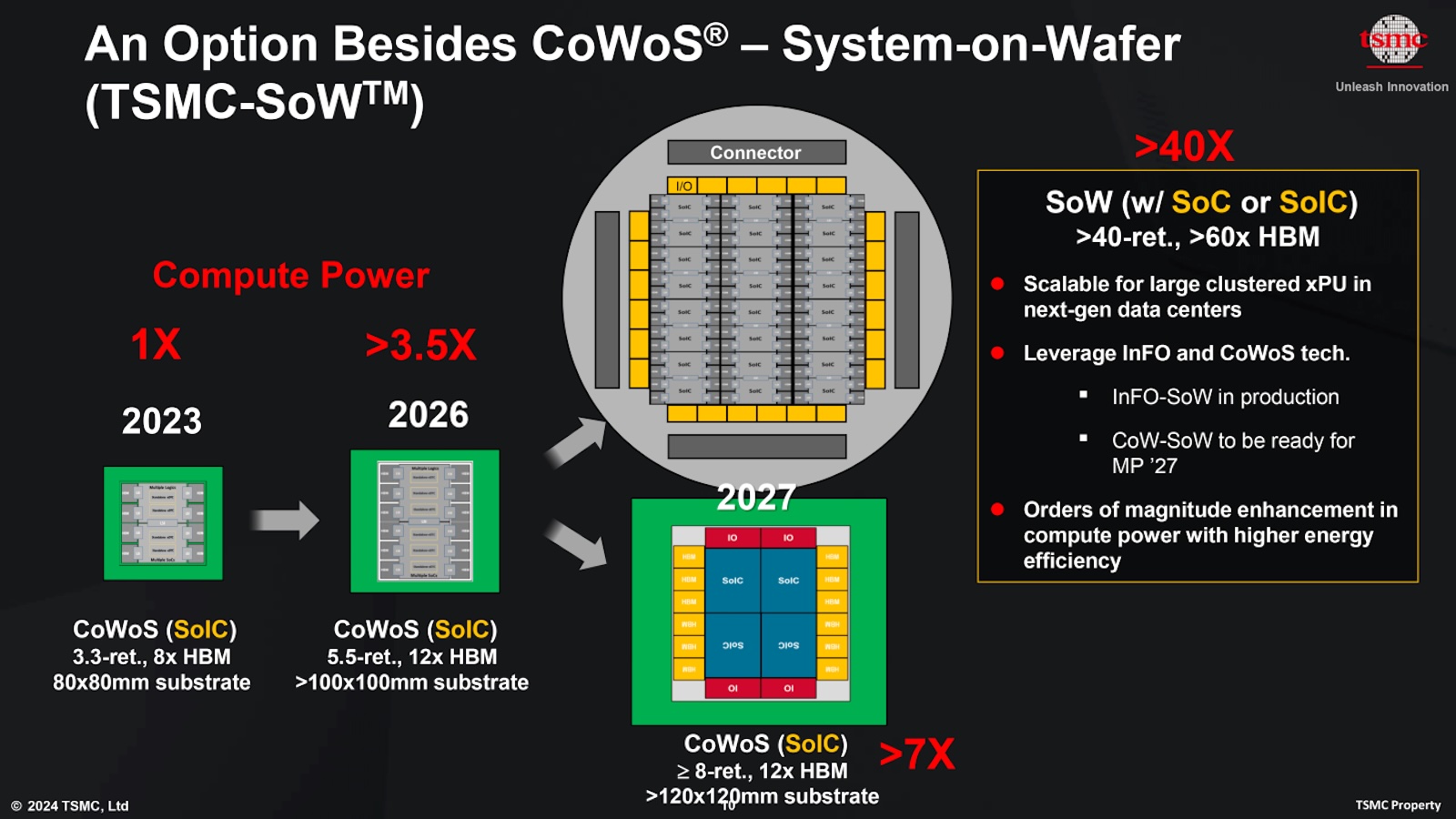
Intel may be starting to capture some of the growth in advanced packaging for artificial intelligence chips, a market dominated by TSMC and its CoWoS technology. The most recent hint comes from the movement of HBM memory from South Korea to Malaysia, where Intel is expanding its advanced assembly and packaging capacity. The data are relevant but should be taken with nuance: they suggest a possible transfer of activity toward Intel, not that TSMC has already lost a quantifiable portion of its market share.
The key points about Intel, TSMC, and AI packaging in 30 seconds
- The demand for AI accelerators is exerting continuous pressure on TSMC’s CoWoS capacity, used to integrate logic chips with HBM memory.
- Data collected by SemiAnalysis Chipbook show $1.3 billion in chip shipments to Malaysia, while shipments to Taiwan drop below $3 billion.
- Intel is expanding its advanced packaging infrastructure there through Project Pelican.
- EMIB and the new EMIB-T enable integration of logic and HBM without using a large silicon interposer.
- TrendForce still ranks TSMC ahead in maturity, manufacturing performance, and integrated services.
This situation highlights how semiconductor manufacturing has evolved with AI. Having the capacity to produce the logic chip no longer guarantees the delivery of the finished accelerators. First, enough HBM memory must be obtained; then all components must be integrated through increasingly complex packaging techniques.
TSMC recognized this problem early and has been increasing its CoWoS (Chip-on-Wafer-on-Substrate) capacity for years. However, demand from Nvidia, AMD, cloud providers, and AI-focused ASIC designers continues to push the need for additional capacity.
This bottleneck is creating an opportunity for Intel Foundry.
$1.3 billion worth of chips shipping to Malaysia
The latest evidence does not come from an announced Intel contract but from trade movement data for semiconductors.
South Korean export data, collected by SemiAnalysis Chipbook, show approximately $1.3 billion in chips sent to Malaysia, while shipments to Taiwan have fallen below $3 billion.
This is interesting because South Korea accounts for a large part of the world’s HBM (High Bandwidth Memory) production, mainly through SK hynix and Samsung.
And HBM is a key component of modern accelerators.
A AI GPU, like those developed by Nvidia, doesn’t only rely on the massive logic chip that performs calculations. Surrounding it are multiple stacks of HBM capable of providing the enormous bandwidth needed to continuously feed the processors.
All these components must be integrated within the same package.
Additionally, Malaysia has a notable advantage: Intel has significant manufacturing, assembly, and testing infrastructure there, which it is expanding for advanced packaging.
Its new complex is part of what is called Project Pelican. According to reports published in 2026, this facility includes die preparation, sorting operations, and support for EMIB and Foveros packaging processes.
Therefore, the increase in memory exports to Malaysia aligns with a possible expansion of Intel’s packaging activity.
But it’s important to note the difference between suspicion and confirmation: trade data alone cannot prove that the entire $1.3 billion is destined for Intel nor identify which accelerators will use this memory.
CoWoS versus EMIB: two ways to build massive AI chips
Advanced packaging has become one of the most crucial technologies in the industry because modern processors are no longer necessarily built as a single silicon block.
Chiplets allow splitting a processor into specialized components, which are then interconnected within the same package.
TSMC and Intel use different approaches to achieve this.
| Technology | Manufacturer | Approach | Role in AI |
|---|---|---|---|
| CoWoS | TSMC | Interposer to connect multiple dies | Widely used in AI accelerators |
| EMIB | Intel | Small silicon bridges embedded in substrate | Connects logic, HBM, and other chiplets |
| EMIB-T | Intel | EMIB with integrated TSVs in the bridge | Designed for higher HBM needs |
| Foveros | Intel | Advanced integration and stacking | Enables 2.5D and 3D systems |
CoWoS uses an interposer that provides high-density connections between components.
EMIB (Embedded Multi-die Interconnect Bridge) avoids using a large silicon interposer under all dies. Instead, Intel places small silicon bridges within the substrate only where high-density connections are needed.
Intel states that EMIB has been in production since 2017 and can be used for both logic-to-logic and logic-to-HBM connections.
The most interesting evolution for the current AI generation is EMIB-T.
This variant incorporates Through-Silicon Vias (TSVs) within the bridge itself. Intel claims this architecture improves power delivery and signal routing required for the next generations of HBM memory.
The company is positioning EMIB-T explicitly for the large chip systems that AI accelerators are beginning to demand.
TSMC still holds a significant advantage
That Intel can benefit from capacity constraints doesn’t mean it has caught up with TSMC.
This distinction is especially important.
TrendForce analyzed in early 2026 the evolution of CoWoS versus EMIB and noted that Intel was expanding its packaging capacity to attract orders from cloud service providers. But it also identified several challenges for the U.S. company.
TSMC maintains an advantage derived from its high manufacturing yields and, above all, its ability to deliver an integrated service.
A customer can build their advanced chips at TSMC nodes and then utilize its packaging infrastructure afterward.
Intel needs to demonstrate that it can offer external customers a competitive alternative with sufficiently high yields at scale.
TrendForce also believes that the market doesn’t necessarily have to become a zero-sum game. The growth in AI demand could be large enough to increase activity for both TSMC and Intel simultaneously.
This nuance significantly changes the interpretation.
Intel doesn’t need to steal TSMC’s main clients to build a meaningful business. It can start by capturing demand that TSMC simply cannot immediately meet.
Intel Foundry’s business might find a different entry point here
For Intel, there’s also a strategic opportunity.
Competing with TSMC solely through manufacturing nodes is extremely challenging. It requires convincing external companies to produce their chips with Intel processes.
Packaging offers an alternative route.
A company can manufacture certain dies at TSMC and then rely on Intel for part of the advanced assembly. Intel itself promotes its packaging infrastructure to integrate chiplets from different technologies and foundries.
This makes packaging potentially a service independent of where each piece is manufactured.
Additionally, Intel has an accumulated advantage: it has been developing integration technologies for decades and has commercially used EMIB for years.
The company is now expanding this experience to turn it into a foundry business.
In 2026, Intel indicated it was close to closing advanced packaging agreements that could represent billions of dollars annually, though this remains a business forecast and not committed revenue contracts.
AI is shifting where the value lies in chip manufacturing
The situation with TSMC and Intel also reflects a much broader change.
For years, much of the semiconductor competition was summarized by nanometer fabrication nodes.
That is increasingly no longer sufficient.
A modern accelerator depends simultaneously on the fabrication process, HBM availability, interconnection technology, substrate, packaging, power consumption, and heat dissipation.
The package has ceased to be just the place where the finished chip is mounted.
Intel describes this transition as moving from a system-on-chip to a system-of-chips. Its EMIB and Foveros technologies are designed around this concept.
AI is accelerating this transformation because it increasingly requires integrating logic and memory in systems that surpass the practical limits of a single die.
That’s why the export data to Malaysia are interesting, even if they don’t yet indicate a radical market share shift.
It may reveal something more fundamental: when the absolute leader lacks sufficient capacity, an alternative technology ceases to be just an alternative and begins to serve as a secondary supply source.
TSMC continues to dominate advanced packaging used by most leading AI accelerators. But Intel has technology, facilities, and expansion plans that precisely match a moment when potential customers need more suppliers.
In a industry limited by HBM, energy, manufacturing, and packaging, having free capacity can become almost as important as having the best technology.
Frequently Asked Questions
Is Intel taking market share from TSMC in advanced packaging?
There are signs that Intel may be gaining new activity while TSMC’s capacity remains under pressure, but available data do not allow quantifying a concrete loss in TSMC’s share.
What is the difference between TSMC CoWoS and Intel EMIB?
CoWoS uses an interposer-based packaging architecture, while EMIB places small silicon bridges within the substrate to connect dies where high density is needed. Both technologies enable integration of logic and high-bandwidth memory.
What is Intel EMIB-T?
EMIB-T is an evolution of EMIB that incorporates TSVs within the silicon bridge. Intel is targeting it for advanced packages with greater power, interconnect, and HBM requirements.
Why is Malaysia important for Intel?
Intel has operated facilities in Malaysia for decades and is expanding its assembly, testing, and advanced packaging capacities there. Project Pelican is prepared to support technologies like EMIB and Foveros.
