
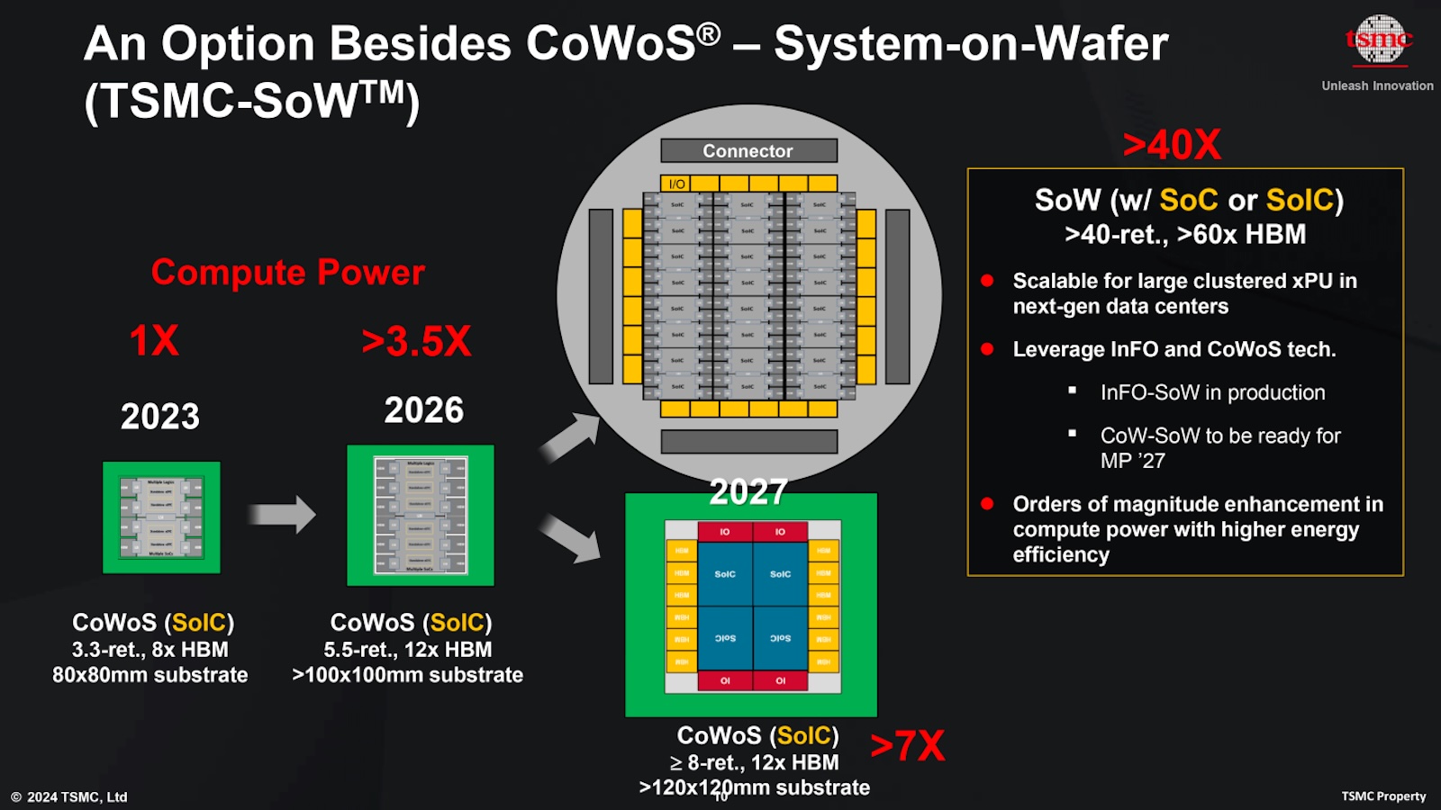
TSMC could take its advanced CoWoS packaging capacity to roughly 260,000 equivalent 300mm wafers a month by the end of 2028, double the roughly 130,000 a month estimated for the end of 2026. The forecast comes from analysts cited by the Taiwanese newspaper Economic Daily News, not from official TSMC guidance, but it reflects a pressure the company itself acknowledges: demand for packaging used in AI accelerators keeps growing faster than available capacity.
The CoWoS expansion in 20 seconds
- Analysts estimate TSMC will go from 130,000 monthly wafers to about 260,000 by 2028.
- The figure is not an official company forecast.
- Arizona and Taiwan’s AP7 plant would account for part of the expansion.
- Intel could reach 40,000 to 45,000 equivalent monthly wafers with EMIB-T in 2028.
- ASE, Amkor, and other suppliers are also benefiting from the shortage.
The figure helps explain how the semiconductor industry’s bottleneck has shifted. Manufacturing a GPU or AI accelerator on an advanced node no longer guarantees the ability to ship the finished product in volume. Large chips need to integrate compute dies with multiple stacks of high-bandwidth memory (HBM), and that integration requires increasingly complex packaging processes.
CoWoS, short for Chip-on-Wafer-on-Substrate, has become one of the central technologies in that chain. NVIDIA is one of its biggest users, and the growth of AI accelerators has repeatedly pushed TSMC to expand its capacity.
The company officially confirms it keeps expanding its advanced packaging facilities to meet demand for artificial intelligence and high-performance computing (HPC). What it hasn’t confirmed is the specific figure of 260,000 monthly wafers for 2028.
CoWoS Has Become Another Critical Piece for Building an AI GPU
A modern data-center accelerator can no longer be understood as a single chip.
Around the compute dies sit several HBM stacks and a complex web of connections that has to deliver huge bandwidth with low latency. The bigger AI models and inference and training workloads get, the more pressure there is to pack more memory and more compute capacity into the same package.
CoWoS is exactly what makes it possible to build these systems through 2.5D integration.
TSMC currently offers three main families: CoWoS-S, CoWoS-L, and CoWoS-R. They don’t all use the exact same architecture. CoWoS-S uses a silicon interposer, CoWoS-L combines a redistribution layer (RDL) with local silicon interconnects, and CoWoS-R uses an RDL-based interposer.
That’s why it’s an oversimplification to describe all of CoWoS as just a big silicon interposer with through-silicon vias (TSVs).
| Technology | General approach | Status |
|---|---|---|
| CoWoS-S | Silicon interposer | In production |
| CoWoS-L | RDL and local silicon interconnect | In production and expanding |
| CoWoS-R | RDL interposer | In production |
| CoWoS 5.5x reticle | Larger packages | Production expected during 2026 |
| CoWoS 14x reticle | Up to about 10 large dies and 20 HBM stacks | Production expected in 2028 |
This last data point does come directly from TSMC.
At its 2026 Technology Symposium, the company said it was already producing CoWoS solutions at 5.5 times reticle size and that it’s preparing a roughly 14x-reticle generation for 2028, capable of integrating around ten large compute dies and twenty HBM stacks.
So the growth in capacity coincides with another trend: every AI package is also getting a lot bigger.
That complicates reading figures expressed simply as monthly wafers. More wafer capacity doesn’t automatically translate into a proportional increase in finished accelerators, because each new generation can consume more area and use different packaging architectures.
From 130,000 to 260,000 Monthly Wafers, According to Taiwanese Analysts
The report published in Taiwan puts TSMC’s capacity at about 130,000 equivalent monthly wafers at the end of 2026, projecting roughly 260,000 by the end of 2028.
If the estimate holds, that would mean doubling it in two years.
Part of the growth would be concentrated at AP7, in Taiwan, and at TSMC’s upcoming U.S. facilities.
TSMC has officially confirmed a major expansion of advanced packaging in Arizona. Its current industrial plan for the state includes six logic wafer fabs, two advanced packaging facilities, and an R&D center, part of an investment program that has reached $265 billion.
In July 2026, it also announced plans to add more fabs for 2nm processes and later technologies, along with additional packaging capacity.
There’s also a logistical reason behind the goal.
Currently, some of the chips made in Arizona need to complete later production stages outside the state. Building a U.S. advanced-packaging supply chain would let more products be manufactured and packaged entirely within the United States.
TSMC doesn’t intend to handle every one of those stages alone.
Its CEO, C.C. Wei, previously explained that the company is working with a major OSAT (Outsourced Semiconductor Assembly and Test) supplier that is building capacity in Arizona on a timeline ahead of TSMC’s own two packaging plants.
The Capacity Crunch Is Creating an Opening for Intel, ASE, and Amkor
The most interesting consequence of the CoWoS bottleneck may be playing out outside TSMC.
According to the analysts cited by Economic Daily News, alternative suppliers such as Intel, ASE, and Amkor are seeing more interest because customers need a second supply chain.
UMC and Vanguard International Semiconductor also show up in specific areas tied to interposers and the fabrication these packages require.
Taiwanese estimates put suppliers outside TSMC at a combined capacity equivalent to around 110,000 monthly CoWoS wafers by 2028.
That doesn’t mean those companies will be manufacturing CoWoS itself.
CoWoS is TSMC’s own technology, and there are different architectures for solving the same problem of integrating large processors, chiplets, and HBM memory.
Intel is probably the most interesting example.
Its alternative is EMIB (Embedded Multi-die Interconnect Bridge) and its newer variants, including EMIB-T. Instead of necessarily using one large interposer spanning the whole package, Intel embeds small, high-density silicon bridges inside the substrate to connect the different components.
Both approaches aim for high-bandwidth integration, but their architecture and manufacturing process differ.
Analysts estimate Intel’s capacity, converted into an equivalent 300mm CoWoS-wafer metric, could evolve as follows:
| Supplier/technology | 2026 | 2027 | 2028 |
|---|---|---|---|
| TSMC CoWoS | ~130,000/month by year-end | — | ~260,000/month |
| Intel EMIB-T equivalent | — | 15,000–20,000/month | 40,000–45,000/month |
| Non-TSMC alternatives combined | — | — | ~110,000/month |
These figures are analyst estimates and equivalences, not official capacity numbers announced by Intel or TSMC. Comparing them directly also calls for caution, since CoWoS and EMIB don’t consume wafers or build packages in the same way.
Google Could Become an Important Piece for Intel
The shortage is fueling another development that could matter for Intel Foundry.
Reports published during 2026 suggest Google is preparing Intel as an advanced-packaging supplier for several million TPUs in 2028.
According to those reports, Google would have reserved capacity for more than three million units, while SK Hynix would be running tests to validate its HBM memory with Intel’s packaging.
These are supply-chain reports and shouldn’t be treated as guaranteed final volumes.
They do show why EMIB could become an important asset for Intel even as the company keeps trying to attract customers to its own manufacturing nodes.
A customer can manufacture the main die at one foundry and turn to a different company for certain packaging stages. Manufacturing and advanced packaging don’t have to go to the same supplier.
For Intel, that opens an additional path into the market for custom AI accelerators.
The AI Race No Longer Hinges Solely on Who Builds the Best Node
For years, a large part of semiconductor competition was explained through nanometers: 7nm, 5nm, 3nm, or 2nm.
Artificial intelligence is forcing everyone to look at a lot more pieces.
An accelerator needs the logic node, but it also needs HBM, interposers or bridges, advanced substrates, packaging, testing, and enough industrial capacity to assemble it all at volume.
A problem at any one of those stages can limit shipments even when there’s plenty of capacity to manufacture the dies themselves.
TSMC acknowledges this pressure and keeps expanding CoWoS. Its technology roadmap also points toward increasingly larger packages: from today’s 5.5x-reticle solutions, to roughly 14x reticles in 2028, and larger sizes starting in 2029.
The 260,000-monthly-wafer forecast lines up with that expansion, but it remains an outside estimate.
What is confirmed is that TSMC is expanding its advanced packaging capacity in Taiwan and the United States while preparing a considerably larger generation of CoWoS for 2028.
And the difficulty meeting all that demand is having an unusual effect in an industry dominated by TSMC: it’s giving Intel, ASE, Amkor, and other suppliers a chance to become real alternatives in one of the most contested parts of the AI supply chain.
via: wccftech
