
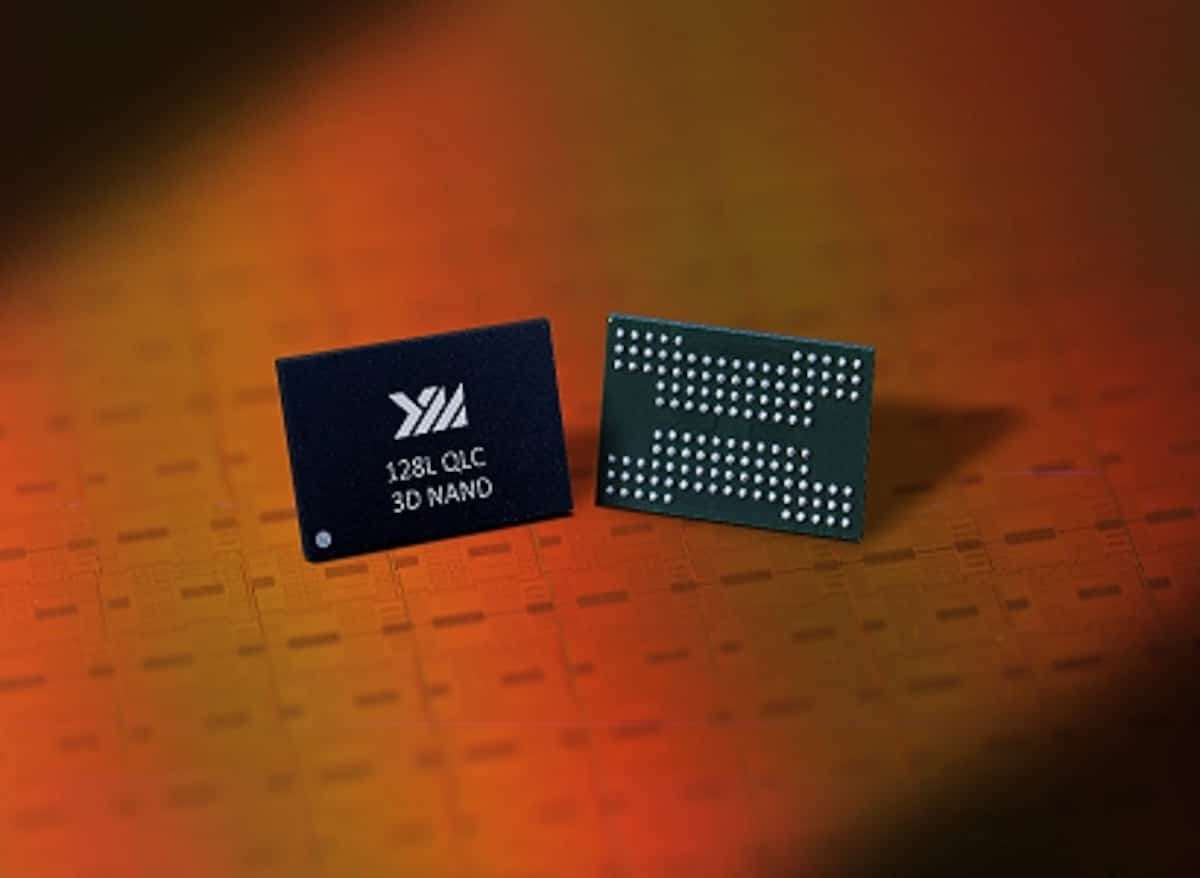
Yangtze Memory Technologies (YMTC), China’s only commercial-scale NAND flash maker, is developing its first low-power DRAM, targeting 9,600 MT/s with a 4F² cell built on a vertical-channel transistor. According to DIGITIMES and research firm Counterpoint Research, the chip is still in development and would only move to mass production at the Wuhan Fab 3 if it clears performance and validation targets.
YMTC’s DRAM push in 20 seconds
- YMTC is working on a 9,600 MT/s LPDDR memory with a 4F² cell and vertical-channel transistor.
- Since October 2025 it has been testing a 16 Gb, 7,500 MT/s LPDDR5 at Fab 2, with no production plans.
- Mass production would depend on validation at Fab 3.
- It remains on the US Entity List and has filed to go public in Shanghai.
The move comes right as Micron has made clear it doesn’t see the 4F² architecture as its next step, a contrast Cloud News covered in YMTC’s broader push to challenge Samsung in enterprise SSDs for AI. YMTC, by contrast, wants to bring the experience it has built with Xtacking, its wafer-bonding technology for NAND, over to DRAM.
Two LPDDR Generations in Parallel
Counterpoint describes two separate workstreams. The first is a second-generation 16 Gb LPDDR5 at 7,500 MT/s that YMTC has been researching and testing at its Fab 2 since October 2025, at a volume of roughly 5,000 wafers a month and without a high-dielectric-constant metal gate (HKMG), a technique commonly used in the fast DRAM made by major manufacturers. The firm stresses that this chip is still in R&D and there are no plans to mass-produce it.
The second workstream has more momentum behind it. It’s a 9,600 MT/s version based on a 4F² cell with a vertical-channel transistor (VCT). DIGITIMES places it as YMTC’s first phase in LPDDR5X, the memory family used in high-end smartphones and, increasingly, local AI devices. Counterpoint calls it LPDDR5, but agrees on the target speed and on Fab 3 as the intended destination, provided the design meets expectations.
On paper, the 4F² cell takes up a third less area than the 6F² cell the industry uses today, because it places the transistor vertically beneath the capacitor. That would allow more bits per wafer without relying on more advanced lithography, a relevant point for a company with limited access to that equipment. The challenge is manufacturing it with good yield, something no maker has yet proven at volume.
Xtacking, YMTC’s Technical Argument
Xtacking manufactures the memory array and the peripheral logic on two separate wafers and then bonds them together. Each part can use whichever process suits it best, and according to Neil Shah, Counterpoint’s vice president of research, that approach lets YMTC keep adding layers using mature lithography tools, an advantage against US export controls. Samsung licensed Xtacking patents in February 2025, a point Counterpoint cites as a vote of confidence in the technology.
Counterpoint also notes that YMTC’s roadmap looks toward 3D DRAM in the long run, with vertically stacked cells. The firm believes that transition will favor companies with wafer-bonding experience, though that’s an analyst forecast and not a company timeline.
More Capacity, an IPO, and Sanctions
The move into DRAM comes at a strong moment for NAND. According to Counterpoint, YMTC was the world’s third-largest maker by shipment volume in the second quarter of 2026, behind Samsung and SK hynix and ahead of Kioxia and Micron. Its NAND revenue share rose from 9% in the first quarter of 2025 to 14% in the first quarter of 2026. The company filed its prospectus to go public on Shanghai’s STAR Market in August 2026, shortly after the debut of CXMT, China’s leading DRAM maker.
On capacity, Reuters reported in April, as covered by Guru3D, a plan to go from roughly 200,000 to roughly 400,000 wafers a month across two new fabs, plus a third plant in Wuhan that would reach around 50,000 wafers a month in 2027 with more than half of its equipment sourced locally. Counterpoint cites a long-term target of around 500,000 wafers a month, DRAM included. The figures come from different sources at different times, so they’re best read as plans rather than installed capacity.
The biggest wildcard remains political. YMTC has been on the US Commerce Department’s Entity List since December 2022, and Counterpoint notes that a bill moving through Congress, the MATCH Act, names it explicitly and targets the deep ultraviolet (DUV) lithography, etching, and deposition equipment its roadmap depends on. For the market, a competitive Chinese DRAM maker would add supply at a time of high prices driven by AI demand, but for now what’s been announced are prototypes and targets.
Frequently Asked Questions
What DRAM memory is YMTC developing?
A low-power memory targeting 9,600 MT/s built on a 4F² cell with a vertical-channel transistor. DIGITIMES describes it as LPDDR5X and Counterpoint as LPDDR5.
When will it start manufacturing it?
There’s no date. According to Counterpoint, it would move to mass production at Wuhan’s Fab 3 only if it completes validation and meets its performance targets.
What’s the advantage of the 4F² cell?
It takes up a third less area than today’s 6F² cell, allowing higher density without relying as heavily on more advanced lithography.
Is YMTC under US sanctions?
Yes. It has been on the Entity List since December 2022, which limits its access to US equipment and technology.
Sources:
