
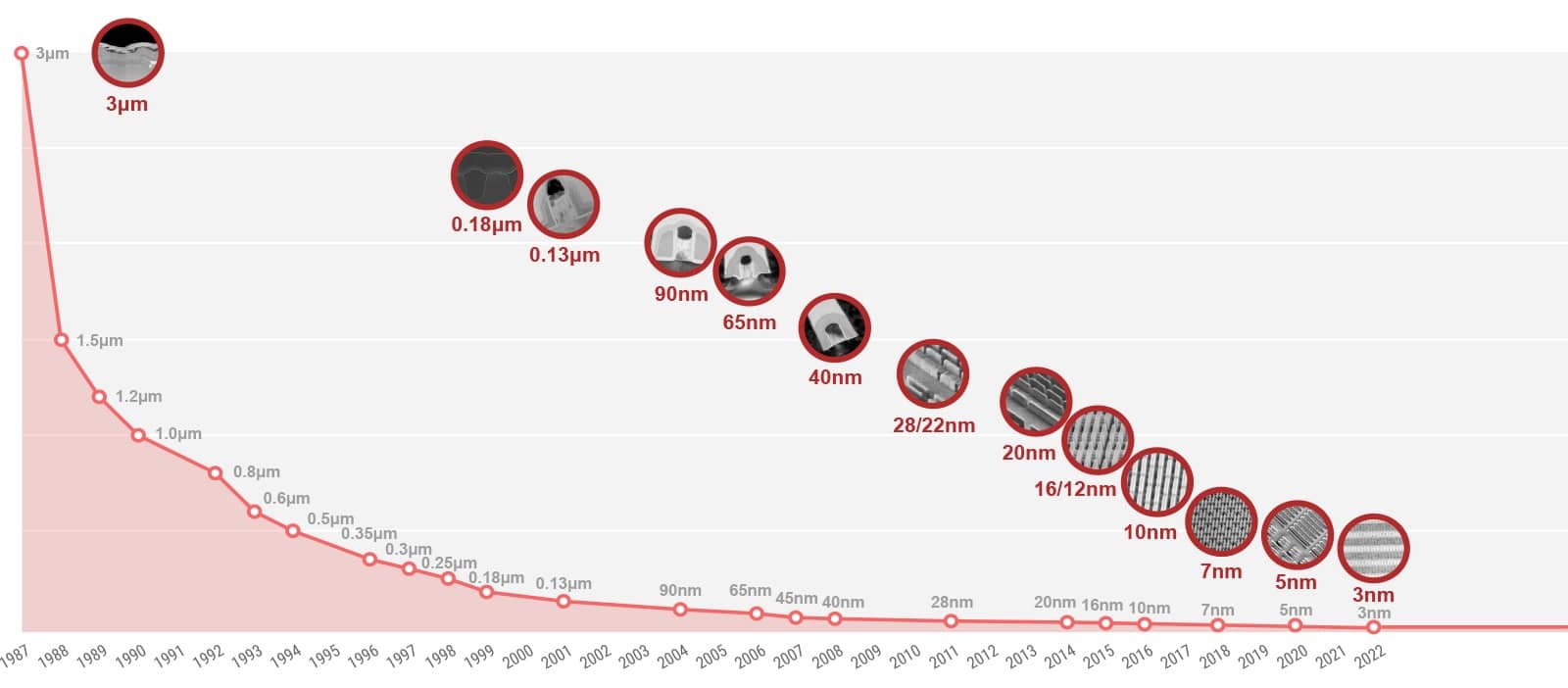
TSMC is reportedly speeding up construction of its new manufacturing complex in Taichung, Taiwan, intended for advanced technologies such as A14, its future generation commercially associated with 1.4 nanometers. Reports out of Taiwan suggest the first fab could be ready ahead of schedule, but one detail calls for tempered expectations: TSMC still officially targets risk production of A14 for 2027 and volume production for 2028.
The key facts on TSMC’s possible A14 acceleration in 20 seconds
- Reports from Taiwan point to faster-than-expected construction of TSMC’s new Taichung fabs.
- The first facility could begin equipment testing during 2027.
- TSMC still officially places A14 at risk production in 2027 and volume production in 2028.
- Samsung, unlike TSMC, does officially maintain its 1.4nm process for 2027 production.
- Finishing a fab earlier doesn’t automatically mean commercial manufacturing moves up too.
The distinction between these two dates is crucial. A fab can finish its structure, receive equipment, and even begin qualifying that equipment months before manufacturing commercial wafers for customers. For now, TSMC hasn’t announced moving A14 up to the second half of 2027, so that possibility should be treated as unconfirmed information, not an official change to its roadmap.
What’s more, TSMC’s latest public statements point precisely in the opposite direction from an already-decided acceleration. On its second-quarter 2026 earnings call, the company reiterated that A14 will start risk production in 2027 and volume production in 2028.
The New Taichung Fabs Could Move Faster Than the A14 Node Itself
The reports published in Taiwan focus on the construction schedule of TSMC’s new Taichung complex.
According to that reporting, the first facility, P1, has apparently progressed quickly through construction and could begin equipment installation and testing during 2027. The following phases, known as P2, P3, and P4, would come online progressively between 2027 and 2028.
That’s a meaningful signal because advanced nodes require enormous industrial infrastructure. But a fab’s completion date and a process’s commercial production date aren’t the same thing.
Before manufacturing customer chips at scale, a fab needs to install lithography, deposition, etch, inspection, and metrology equipment; calibrate hundreds of process steps; validate designs; complete intellectual-property libraries; and reach yields that make volume wafer production economically viable.
TSMC has already made significant progress on that last part.
During its July earnings report, the company said its internal product-like test vehicles had reached close to 90% device yield and around 90% yield on 256 Mb SRAM. It also said customer tape-out activity was running ahead of its internal schedule, continuing a pattern already visible in TSMC’s faster-than-planned 2nm ramp-up.
Those are promising figures, but even after sharing them, TSMC continued to place volume production in 2028.
| Technology | Official schedule |
|---|---|
| TSMC N2 | Volume production started in Q4 2025 |
| TSMC N2P | Production expected in H2 2026 |
| TSMC A16 | Production expected in H2 2026 |
| TSMC A14 | Risk production in 2027 |
| TSMC A14 | Volume production in 2028 |
| Samsung SF1.4 | Production expected in 2027 |
TSMC describes A14 as a full-node jump from N2, and it will use the company’s second generation of nanosheet transistors.
The company estimates the process can deliver 10% to 15% more performance at the same power, or cut power consumption by 25% to 30% at the same performance. It also expects roughly 20% higher chip density than N2. These are TSMC’s own technical targets, not independently verified results from commercial products.
Samsung, Not TSMC, Is the One Officially Holding to 1.4nm for 2027
An eventual A14 acceleration would have a curious side effect: it would bring TSMC’s schedule closer to the one Samsung has been announcing for years.
Samsung laid out its intention to manufacture chips on a 1.4nm process by 2027 back in 2022. Two years later, it reaffirmed that target at its Foundry Forum and said SF1.4 development was on track with its performance and yield goals.
So claiming that a hypothetical 2027 A14 from TSMC would automatically put Samsung “against the ropes” oversimplifies the situation.
On paper, Samsung is aiming to arrive that very same year.
Samsung is also developing SF2Z, an evolution of its 2nm process that incorporates BSPDN (Back Side Power Delivery Network), a power-delivery scheme routed from the back side of the wafer. Its production is scheduled for 2027 and is aimed especially at high-performance computing and artificial intelligence.
The challenge for Samsung will be turning its technology roadmap into production that’s competitive on performance, power, density, wafer yield, cost, and available capacity for customers.
Those parameters matter far more than the marketing number attached to the node.
Terms like 1.4nm, 14A, or A14 don’t represent a directly comparable physical dimension across manufacturers. Each company uses its own naming scheme, and two processes that appear to belong to a similar generation can have very different characteristics.
Intel 14A Is Also in the Race, With High-NA EUV
Intel is the third major participant in this race.
Its future Intel 14A platform is closely tied to High-NA EUV lithography and the dual power-delivery approach Intel is building into its 1.4nm process roadmap, a technology Intel has been working on with ASML for years.
The company announced this same week that it has already processed more than a million wafers using High-NA EUV, across equipment certification, research, development, and production on certain layers of some Panther Lake processors.
That figure doesn’t mean Intel 14A is already in commercial production either. It shows the level of industrial experience Intel is building up with a lithography technology that will carry more weight in future generations.
The competition between TSMC, Samsung, and Intel will therefore be considerably more complex than checking who puts “1.4nm” on a slide first.
| Manufacturer | Next advanced generation | Highlights |
|---|---|---|
| TSMC | A14 | Second-generation nanosheet, NanoFlex Pro |
| Samsung | SF1.4 | Evolution of its GAA architecture |
| Intel | 14A | High-NA EUV and evolution of RibbonFET/PowerVia |
For TSMC, actually moving A14 up could carry commercial value, because customers start preparing their chips long before a technology enters production.
Apple — which has already set its sights on 1.4nm chips — NVIDIA, and AMD are among TSMC’s biggest customers, but there’s no official confirmation of specific products from these companies being manufactured on A14. Linking the supposed acceleration to specific future processors would, for now, be speculative.
What TSMC has confirmed is that it’s seeing strong customer interest in A14, both for smartphones and for high-performance computing and AI applications.
And this is probably the most interesting detail in all the reporting out of Taiwan.
TSMC doesn’t necessarily need to publicly move A14 from 2028 to 2027 to benefit from finishing part of its infrastructure early. Having fabs and equipment ready ahead of time can provide more room to run risk production, improve yields, qualify processes, and respond to demand once volume ramp-up begins.
TSMC itself acknowledges that A14 development is progressing well and its yield results are ahead of plan, while new customer design activity is also running ahead of schedule.
That makes it plausible that certain phases could progress faster than initially expected. But as of September 10, 2026, the public schedule remains unambiguous: A14 risk production in 2027 and volume production in 2028.
If TSMC ends up carrying the Taichung construction acceleration over into its commercial schedule, that would meaningfully change the race against Samsung and Intel. Until the company officially revises its dates, presenting TSMC’s 1.4nm as a commercial reality for 2027 gets ahead of the data currently available.
