
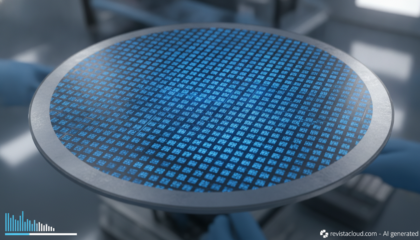
TSMC will unveil in December a high-density SRAM memory cell under 0.017 µm2 built on its A14 process, the first real reduction in this cell’s size since 5nm, where it had stalled at 0.021 µm2 in 2020. The work will be presented at the IEDM 2026 conference in San Francisco and, according to its abstract, is the smallest SRAM cell published to date. The A14 node remains on track for volume production in 2028.
The A14 node’s SRAM in 30 seconds
- TSMC will present a high-density SRAM cell under 0.017 µm2 on December 14 at IEDM 2026.
- Since N5, in 2020, the cell had stalled at 0.021 µm2, also on N3E and N2.
- Versus N2, TSMC promises A14 will deliver 10% to 15% more speed or 25% to 30% lower power.
- Chip density improves by around 20%, with volume production arriving in 2028.
The figure matters because SRAM, the fast memory that forms the caches of processors, GPUs and AI accelerators, had gone years without shrinking at the same pace as logic. Revista Cloud has already explained what SRAM is and how it differs from DRAM and flash. If compute transistors keep getting smaller while the cache doesn’t, the cache ends up taking up an ever-larger share of the chip, and every square millimeter of silicon on an advanced node is expensive.
Eight years with the SRAM cell stuck
According to Hardware Busters, TSMC’s high-density 6T cell measured 0.021 µm2 on N5, the 5nm process from 2020. N3 trimmed it slightly, but the dominant variant, N3E, went back up to 0.021 µm2. N2, the 2nm process that introduced nanosheet transistors, kept the same cell size. N2’s density gain, around 38.1 Mb/mm2, roughly 10% more according to a paper presented at ISSCC 2025, came from the circuitry surrounding the cell: nanosheets allow 512 cells per bit line to be connected instead of 256.
With A14, the cell drops below 0.017 µm2, at least 19% smaller than on N5. TSMC’s paper abstract, authored by Shien-Yang Wu and Chih-Hao Chang, attributes the improvement to scaling the dimensional design rules and also claims the highest SRAM macro density published to date. The competition is at the same starting point: the high-density cell on Intel’s 18A process also measures 0.021 µm2.
What A14 promises over N2
The paper, titled “A14 CMOS NanoFlex Pro Platform Technology with 2nd Gen. Nano-sheet and Full Node PPA Benefits for HPC/AI and Mobile SoC Applications,” will be presented on Monday, December 14, according to the program listed on SemiWiki. TSMC describes A14 as a full node improvement: 10% to 15% more speed at the same power, or 25% to 30% lower power at the same speed, versus N2. Chip density, combining logic and SRAM, increases by around 20%.
The work also includes packaging technologies: through-silicon vias (TSVs), a redistribution layer enabling a 4.5 µm bump pitch in SoIC, TSMC’s 3D chip integration, and high-performance MiM capacitors. TSMC mentions robust manufacturing yield, but the abstract gives no figures.
The first version of A14 will keep front-side wafer power delivery; the Super Power Rail variant, with back-side power delivery, will arrive roughly a year later. Revista Cloud already reported that TSMC may be speeding up its A14 node, something the company hasn’t confirmed, and that design tool makers such as Cadence have already certified their tools for A14.
A lab figure, not a product spec
This figure needs careful reading. The 0.017 µm2 size corresponds to a test structure, not a product spec. A cache’s real density also depends on its periphery, the assist circuits, and the operating voltage, and high-performance level-1 and level-2 caches use larger cells than the high-density one. Hardware Busters estimates that the first processors and GPUs built on A14 won’t arrive before 2029, and notes that a 20% density gain is a modest improvement for a full node, on wafers that will be expensive.
Even so, the return to SRAM scaling matters for AI and data center chip design, where cache takes up an ever-growing share of die area. Manufacturers such as AMD have turned to stacking cache on top of the processor, as in its X3D models, or moving it to separate chiplets. A smaller cell doesn’t eliminate those techniques, but it gives designers a bit more room on the main die.
Frequently asked questions
What has TSMC achieved with A14’s SRAM?
A high-density SRAM cell under 0.017 µm2, at least 19% smaller than on N5, which it will present at the IEDM 2026 conference.
When will chips be built on A14?
TSMC expects volume production in 2028. According to Hardware Busters, the first processors and GPUs on A14 won’t arrive before 2029.
What does A14 improve over N2?
According to TSMC, 10% to 15% more speed or 25% to 30% lower power, and around 20% higher chip density.
Why hadn’t SRAM shrunk since N5?
The cell stayed at 0.021 µm2 on N5, N3E and N2; N2’s density gains came from the circuitry around the cell, not the cell itself.
Sources:
