
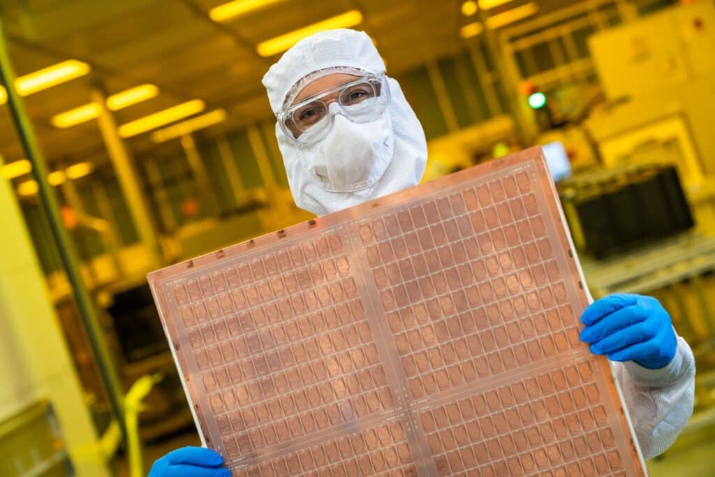
Samsung Electro-Mechanics, known as Semco, has completed the first reliability tests on its 100 × 100 millimeter glass substrates and has moved into a new validation phase using customer chips. The advance brings the project closer to one of the most demanding stages of development: checking how the semiconductor package behaves as a whole, not just the substrate on its own. The South Korean company aims to get a production line for this technology up and running before the end of 2027, although it still has to pass customer testing and solve the industrial challenges of large-scale manufacturing.
Key facts about Samsung’s glass substrates in 30 seconds
- Samsung Electro-Mechanics has finished the first reliability tests on its 100 × 100 mm glass substrates.
- The next phase brings in customer chips to check how the full package behaves.
- The designs under development include more than 20 circuit layers and more than 80 integrated passive devices.
- The technology aims to reduce warpage and improve the electrical characteristics of packages for AI accelerators.
- The company is targeting a production line before the end of 2027, but commercialization depends on technical and industrial validation.
The phase change comes as artificial intelligence (AI) accelerators and data center processors demand ever-larger packages with more electrical connections. In these designs, the substrate must maintain the mechanical stability and electrical properties needed to connect high-performance chips, memory, and other components within the same package.
Glass is emerging as an alternative to the organic materials typically used in packaging substrates. Its rigidity and dimensional stability can help control warpage in large structures, although turning those properties into an industrial advantage requires solving manufacturing, reliability, and production-yield problems.
From Testing the Substrate to Validating the Full Package
According to reports published by South Korean media, Samsung Electro-Mechanics has already completed the initial reliability tests on the substrate and is now verifying how the package behaves after mounting customer chips. The company also maintains development partnerships with several international firms.
The difference between the two stages matters. A substrate can pass mechanical and electrical tests on its own and still run into problems once it’s integrated with a semiconductor. Mounting introduces new stresses and differences in thermal behavior between materials, so the reliability of the whole assembly needs to be checked.
Validation has to determine whether the structure keeps its properties when the package is subjected to expected operating conditions. In AI systems, temperature swings and power delivery demands can test both the materials and the connections between layers.
Samsung Electro-Mechanics is working with 100 × 100 millimeter glass substrates. The designs described by the South Korean press include more than 20 circuit layers and more than 80 integrated passive devices, known as IPDs. These components can perform functions such as stabilizing power delivery or conditioning signals.
The substrate’s surface area also matters. As a reference point, the package for the NVIDIA Blackwell GPU cited by trade media measures roughly 81.5 × 74.8 millimeters. A 100 × 100 millimeter substrate offers more surface area, although comparing dimensions alone isn’t enough to determine the two designs’ performance or their compatibility with the same manufacturing process.
Integrating more layers and connections over a large surface raises the precision requirements. Manufacturers have to control circuit formation, the holes drilled through the glass, metal fill, and the stability of the assembly during manufacturing and mounting.
Why Glass Interests AI Chipmakers
Packaging substrates connect the semiconductor to the circuit board and distribute signals and power. They’re already an important component in conventional processors, but their complexity grows when a single package brings together several compute chips, high-bandwidth memory, and other elements.
AI accelerators have raised these demands. The growing number of connections and package sizes forces better control over warpage and circuit precision. If the substrate loses stability during manufacturing or operation, problems can appear in the connections and in the assembly’s reliability.
Samsung Electro-Mechanics argues that glass offers advantages over conventional organic materials thanks to its lower thermal expansion and dimensional stability. These properties can help reduce warpage and favor designs with denser connections. The company has shown its progress in glass substrates at the KPCA Show 2026, alongside other packaging technologies for accelerators, servers, and data centers.
Using glass also raises difficulties. It requires drilling fragile materials with great precision, creating reliable conductive vias, and avoiding cracks during processing. Moreover, the material’s theoretical advantages only translate into a competitive product if the manufacturer manages to keep quality consistent and defect rates low enough.
That’s why validating with real chips marks a different step from showing off prototypes. It makes it possible to check the behavior of a structure much closer to the final product, although it doesn’t by itself confirm that the technology is ready for mass production.
Production Targeted for Late 2027, With Challenges Still Ahead
Reports published in early October place Samsung Electro-Mechanics’ goal of launching a glass substrate production line before the end of 2027. The company is developing the technology with international customers and has moved from sample validation to testing the full package.
That timeline should be read as an industrial target, not a confirmed date for widespread commercial availability. Customer testing, design qualification, and the ability to manufacture at adequate yields could all shift the schedule.
The process has also run into difficulties in evaluations of modules with through-glass vias, known as TGV (Through-Glass Via). In September, DIGITIMES reported that evaluation of these modules sent to TSMC was taking longer than expected, affecting the schedule for certain equipment orders. The new phase of testing with customer chips reflects progress in development, but doesn’t prove that every earlier validation has concluded successfully.
Samsung Electro-Mechanics is also strengthening its access to the materials needed to manufacture these substrates. In November 2025, it announced a memorandum of understanding with Sumitomo Chemical Group to create a joint venture dedicated to glass core material. The initiative aims to combine both companies’ capabilities to develop the supply of an essential component for this technology.
The race for glass substrates isn’t limited to South Korea. Japanese manufacturers such as Shinko Electric Industries and Dai Nippon Printing are also working on this technology and have made progress developing multilayer structures and manufacturing processes. The competition will be decided both by the designs’ specs and by the ability to produce them reliably and at a reasonable cost.
For Samsung Electro-Mechanics, moving to validation with customer chips brings the project closer to a test that’s more representative of real-world use. The next challenge will be demonstrating that the substrate can meet the demands of the package and that the manufacturing process can maintain the quality needed to serve accelerator and server makers.
Frequently Asked Questions
What are glass substrates for semiconductors?
They’re packaging substrates that use glass as the core material instead of conventional organic materials. Their dimensional stability and thermal properties can prove useful in large packages with high-density connections.
What is Samsung Electro-Mechanics testing?
The company has completed the first reliability tests on its 100 × 100 millimeter substrates and has moved to validating packages with customer chips. This phase makes it possible to study how the whole assembly behaves, not just the substrate on its own.
When could glass substrate production start?
Reports published in October 2026 place the target of launching a production line before the end of 2027. The date depends on technical validation and industrial preparations.
Why are these substrates of interest for artificial intelligence?
AI accelerators integrate high-performance chips and need large packages with numerous electrical connections. Glass can help reduce warpage and improve dimensional stability, although it still has to prove its reliability and industrial viability.
