
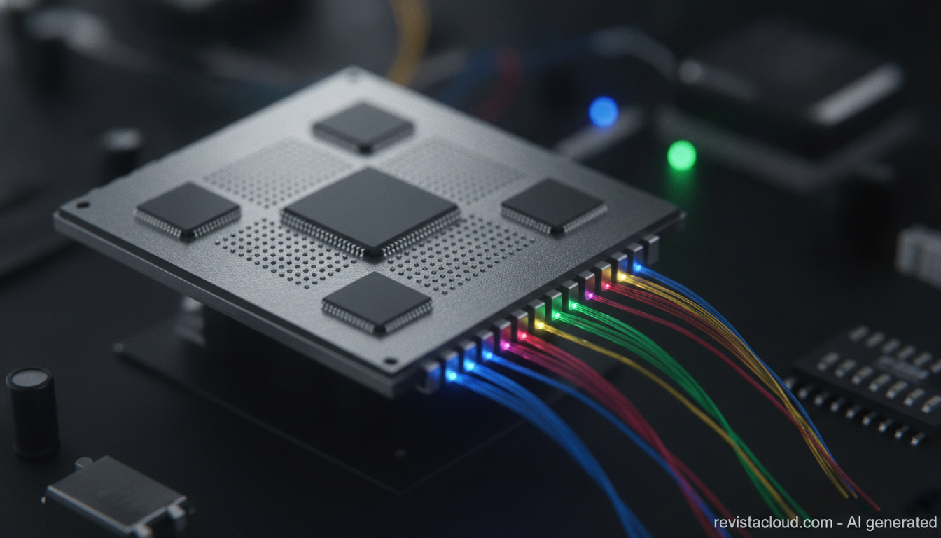
NVIDIA has shown a prototype that places optical engines directly on the silicon interposer — the piece that holds and connects the GPU to its memory — instead of on the organic substrate of the package, as its current co-packaged optics (CPO) switches do. Researcher Nikola Nedovic presented it at SEMICON West 2026 in San Francisco, along with a wavelength-division multiplexing demo reaching 256 Gb/s per fiber. The company itself places it at the research stage and hasn’t given a commercialization date.
NVIDIA’s optics-on-interposer in 30 seconds
- NVIDIA calls it Optics-on-Interposer (OOI): moving optical engines from the organic substrate to the silicon interposer, next to the compute chips.
- It already has prototypes, but hasn’t published bandwidth-density or power figures.
- A DWDM demo combined eight 32 Gb/s wavelengths to reach 256 Gb/s per fiber.
- Both technologies remain in research, behind the CPO switches NVIDIA already mass-produces.
The talk, titled “Optical Integration for the Next Generation of AI,” was held on October 13 and first covered by Korean outlets like The Elec. Nedovic explained that NVIDIA is proposing and evaluating technologies for future products, and that the company is working to solve the problems that currently keep them from reaching commercialization. The idea isn’t new for him: in February 2023, he co-authored a paper with Ben Lee, Trey Greer, and Tom Gray in the Journal of Lightwave Technology titled “Beyond CPO,” which already argued for bringing optics onto the interposer as the next step once CPO falls short for accelerated computing.
From the Substrate to the Interposer: What Changes
In co-packaged optics, the modulators and photodetectors that convert the electrical signal into light sit in the same package as the network chip, instead of in pluggable transceivers at the front of the switch, while the lasers move to external modules. That’s what NVIDIA already sells with Quantum-X Photonics, for InfiniBand networks with optical engines mounted on sockets, and Spectrum-X Photonics, for Ethernet, with soldered engines and detachable fiber connectors. In both cases, the electrical signal leaves the chip, crosses the interposer, and then the organic substrate before reaching the optical engine.
OOI removes that last leg. The optical engines sit on the interposer itself, so the signal travels over its short, fine-pitch connections — the same way it does today between the GPU and HBM memory. According to NVIDIA, that would allow higher bandwidth density and lower power consumption, though the company hasn’t given figures. One of the diagrams from the talk, captured by Wccftech, illustrates the difference in scale for a package built for a 200 Tb/s ASIC: about 100 millimeters on the organic substrate versus about 8 on the interposer. In exchange, the design complicates thermal management and packaging, and Nedovic stressed that a full supplier ecosystem is needed for CPO to reach mass production.
More Data Per Fiber With DWDM
The second piece is dense wavelength-division multiplexing (DWDM), which sends several data streams over the same fiber using different colors of light and separates them at the receiver. In NVIDIA’s demo, eight wavelengths at 32 Gb/s each added up to 256 Gb/s per fiber. The technique is common in long-haul networks, but bringing it inside an AI chip’s package, with very precise lasers and filters, is a different challenge. It’s also still in the research stage.
What’s Already in Production, and What’s Next
It’s worth separating the prototype from what NVIDIA already sells. Its Spectrum-X Ethernet Photonics switches, with CPO over 200 Gb/s SerDes for the Vera Rubin platform, are in full production, and the company says they use four times fewer lasers and consume five times less power than a network with pluggable transceivers. Early customers include CoreWeave, Lambda, and Oracle Cloud Infrastructure. Behind them is a broad supply chain, with TSMC handling silicon-photonics manufacturing and its COUPE packaging technology, SPIL on assembly and testing, and Coherent, Lumentum, and Sumitomo Electric supplying the external lasers.
The next known stop is Feynman, NVIDIA’s architecture planned for 2028, which already points to CPO optics and that the company wants to pair with Kyber NVL1152, an architecture that links eight racks into a single, 1,152-GPU NVLink domain. NVIDIA hasn’t said whether OOI will arrive with Feynman or later. What the talk does make clear is that the company is already working on the step that would come after today’s CPO, whose fundamentals CloudNews covered in this analysis of how CPO brings fiber to the chip.
Frequently Asked Questions
What is Optics-on-Interposer (OOI)?
It’s NVIDIA’s name for placing optical engines on the silicon interposer that holds the compute chips, instead of on the organic substrate of the package.
When will OOI reach NVIDIA products?
There’s no date. NVIDIA has prototypes, but the technology is still in research and the company only says it’s evaluating it for future products.
What speed did the DWDM demo reach?
256 Gb/s per fiber, combining eight wavelengths of 32 Gb/s each.
Does NVIDIA already sell switches with co-packaged optics?
Yes. Quantum-X Photonics for InfiniBand and Spectrum-X Photonics for Ethernet, the latter already in full production for the Vera Rubin platform.
Sources:
- The Elec: Nvidia Unveils Next-Generation CPO Technology
- NVIDIA Research: Beyond CPO, a motivation and approach for bringing optics onto the silicon interposer (2023)
- TrendForce: NVIDIA Unveils Next-Gen CPO Prototype With Optics on Silicon Interposer
- Wccftech: NVIDIA’s Next-Gen CPO Technology Puts Optics Directly On The Interposer
- StorageReview: NVIDIA Spectrum-X Ethernet Photonics enters full production
