
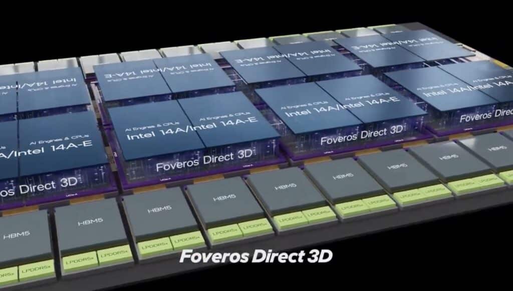
Intel’s 14A manufacturing process is being evaluated by some of the world’s largest tech companies, according to a Piper Sandler research note picked up by Wccftech. Amazon, Apple, AMD, Google, Tesla, Microsoft, Nvidia and Qualcomm are reportedly among the companies studying Intel’s next-generation node, although the U.S. company has not yet announced a major external customer for 14A.
Key facts about Intel 14A and its potential customers, in 30 seconds
- Piper Sandler says eight major tech companies are evaluating the 14A process.
- Intel has set 14A’s risk production for the second half of 2027.
- High-volume production is committed for 2028.
- Intel says defect density and transistor performance trends are ahead of 18A’s trajectory at a comparable stage.
- The node incorporates PowerDirect and the second generation of RibbonFET transistors.
The interest comes as Intel tries to strengthen its third-party manufacturing business and narrow the technology gap with TSMC. The company has confirmed that 14A will move forward toward risk production in 2027 and high-volume manufacturing in 2028, while it continues working to attract external customers.
Piper Sandler’s information does not amount to signed contracts. A company evaluating a manufacturing process means it is analyzing its technical characteristics and possible use, but it does not confirm that it will manufacture commercial products with that node.
Intel 14A Improves Its Metrics Ahead of Production
One of the arguments used to explain the interest around 14A is the evolution of its defect density. This metric, known as D0, measures the number of defects per unit of surface area on a silicon wafer. As a process matures, reducing defects typically helps improve manufacturing yield and the number of usable chips per wafer.
Intel has said that 14A is advancing in defect density and transistor performance ahead of 18A’s trajectory at a comparable stage. During its second-quarter earnings presentation, CEO Lip-Bu Tan said 14A’s PDK 0.5 was already complete and that PDK 0.9 was expected in October.
A PDK, or process design kit, gives designers the rules and models needed to develop circuits for a specific manufacturing technology. Its progress matters to external customers because it lets them start adapting their designs to the process.
Some reports published in recent weeks put 14A’s D0 at around 0.5 in June 2026, with a target of between 0.1 and 0.2 for the first quarter of 2027. These figures come from third-party reports and are not a complete official performance table published by Intel, so they should be read as reported data rather than definitive commercial specs.
Intel itself has confirmed the process’s relatively strong performance. Tan said performance and defect-density metrics were beating the company’s expectations and that Intel was preparing 14A for broader customer adoption.
Amazon, Apple, AMD, Google, Tesla, Microsoft, Nvidia and Qualcomm
The list attributed to Piper Sandler includes Amazon, Apple, AMD, Google, Tesla, Microsoft, Nvidia and Qualcomm. These are companies with very different needs, but all of them rely to some degree on advanced semiconductors for processors, accelerators, devices or infrastructure.
Evaluating a node doesn’t mean all of them will become Intel Foundry customers. The usual process can include testing electrical characteristics, design libraries, performance, power consumption, density, costs and production capacity before deciding whether a specific product can be manufactured with that technology.
Intel has publicly discussed rising interest from external customers. In its latest earnings presentation, Tan said the company was seeing greater engagement from foundry customers and expected that delivering new PDK versions and performance data would help move those projects forward.
For now, Intel has not publicly identified any of these eight companies as a confirmed production customer for 14A. That distinction matters a great deal when assessing the node’s commercial status.
The company also maintains significant internal demand. During its earnings presentation, Intel explained that rising demand for its own products, together with progress with external customers, supported its decision to commit to ramping up 14A’s high-volume production in 2028.
PowerDirect and RibbonFET 2 Are Two of 14A’s Technologies
Intel 14A belongs to the class of manufacturing processes the company calls 1.4nm. As with other advanced-node brand names, this figure should not be read literally as a single physical transistor dimension.
The process incorporates PowerDirect, a backside power delivery technology. The idea is to separate the interconnects used to deliver power from the front-side interconnects mainly used for signals, with the goal of reducing certain electrical limitations and improving density.
14A also introduces RibbonFET 2, the second generation of Intel’s Gate-All-Around (GAA) transistor architecture, first used in the 18A node that powers Panther Lake. This design wraps around the transistor channel to improve electrical control as its dimensions shrink.
These technologies are part of Intel’s technical pitch for 14A, but the node’s commercial success will also depend on factors such as performance, power consumption, costs, manufacturing capacity and wafer yield.
Intel Sticks With 2028 for High-Volume Production
Intel’s official timeline puts 14A’s risk production in the second half of 2027 and high-volume manufacturing in 2028. In July, Tan explained that the company had decided to commit to the high-volume ramp-up during 2028.
At the same time, some recent reports have pointed to a possible pull-forward within that timeline due to the evolution of defect density. These are external estimates, not a change Intel has announced to its official schedule. The company still publicly cites 2028 as its reference point for the high-volume ramp-up.
The development of 14A is also tied to the investments Intel will need to make to increase manufacturing capacity. Recent reports suggest that equipping additional capacity at Fab 62 could require around $10 billion to reach roughly 20,000 wafers a month, though that figure comes from external estimates and should not be confused with an officially confirmed budget for the entire project.
The company also carried out a major capital raise in August. However, directly linking that money to a specific 14A customer would go beyond what has been publicly confirmed.
The interest described by Piper Sandler, then, comes at a stage that still precedes the node’s commercial consolidation. Intel has a defined production timeline, has reported technical progress and says it is holding talks with external customers. But the decisive question will be which companies move from evaluating the node to committing to specific products and volumes.
For Intel Foundry, 14A also represents a test of its ability to attract advanced third-party designs. Evaluation by major companies can expand commercial opportunities, but there is still a process of validation, design and contracting between a technical evaluation and mass production.
Frequently Asked Questions
Which companies are evaluating Intel 14A?
According to the Piper Sandler note picked up by Wccftech, Amazon, Apple, AMD, Google, Tesla, Microsoft, Nvidia and Qualcomm are evaluating the process. Evaluation does not mean these companies have signed production contracts with Intel.
When will Intel start producing 14A?
Intel is keeping risk production set for the second half of 2027 and has committed to starting the high-volume manufacturing ramp-up during 2028.
What technologies does Intel 14A use?
14A incorporates PowerDirect, the backside power delivery system, and RibbonFET 2, the second generation of Intel’s Gate-All-Around transistors.
Does Intel already have a major confirmed customer for 14A?
The information available does not publicly identify a confirmed major external customer for 14A production. Intel has reported rising interest and talks with external customers while it continues preparing the process for high-volume production.
