
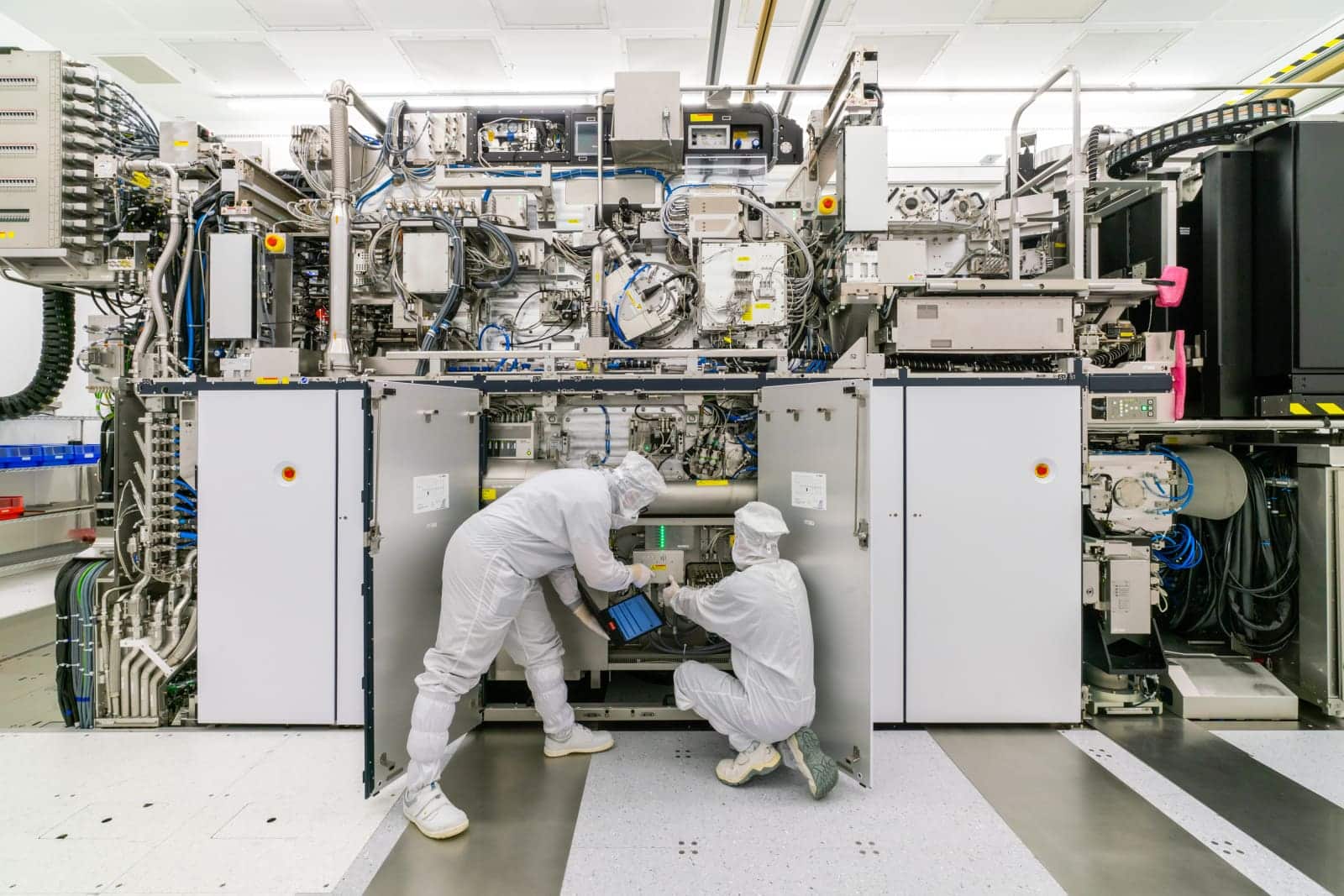
Intel Foundry has begun manufacturing some of its Intel Core Ultra Series 3 processors, known as Panther Lake, using ASML’s High-NA EUV machines on specific layers of the Intel 18A process. This makes the manufacturer the first to ship a high-volume logic product with this new lithography generation, although most of the chip still relies on conventional EUV equipment.
The key points of High-NA EUV in Panther Lake in 30 seconds
- Intel utilizes High-NA EUV on some layers of Panther Lake fabricated with Intel 18A.
- Yields achieved match those of conventional EUV NXE machines, according to ASML.
- Production does not rely solely on High-NA: layers are qualified on both platforms.
- The technology improves resolution and can reduce the need for multiple exposures.
- TSMC still questions its cost, while Samsung moves forward without announcing an equivalent product in production.
This announcement represents a significant commercial milestone for ASML. The Dutch company had installed its first High-NA machines in research centers but needed to demonstrate they could be integrated into a real fab, maintain adequate availability, and achieve yields comparable to a mature platform.
Intel has not specified how many Panther Lake layers use High-NA EUV, what percentage of processors go through these machines, or the absolute performance of the process. ASML only indicates that certain layers of Intel 18A have achieved double qualification in Oregon and that products produced with them are already being shipped to customers.
Intel hasn’t moved all of Panther Lake to High-NA
The phrase “manufactured with High-NA EUV” might give a mistaken impression. Panther Lake is not entirely produced with the new TWINSCAN EXE machines. Intel uses High-NA on a selected set of layers, while maintaining the conventional NXE platform with standard numerical aperture for the rest of the process.
Double qualification means a single layer can be manufactured either with High-NA EUV equipment or with the existing NXE machines. The company claims to have matched performance between both options, allowing them to introduce the new technology without making it a single point of failure for the process.
| Element | Situation in Panther Lake |
|---|---|
| Manufacturing process | Intel 18A |
| Product | Part of Intel Core Ultra Series 3 |
| Codenamed | Panther Lake |
| Use of High-NA EUV | Selected layers |
| Alternative platform | Conventional ASML NXE EUV |
| Qualification type | Double qualification EXE-NXE | Declared performance | Equalized between both platforms |
| Location | Intel facility in Oregon |
| Exact volume | Not disclosed |
| Number of High-NA layers | Not disclosed |
This approach reduces industrial risk. Intel can gather operational data—such as exposure times, maintenance needs, defect rates, and stability—without redesigning the entire Intel 18A around a relatively new machine.
It also allows continued production on its existing fleet if a High-NA machine undergoes maintenance or stops. In a semiconductor fab, maximum resolution doesn’t help much if equipment’s availability, layer-to-layer accuracy, and wafer throughput are compromised.
In 2024, Intel received the first commercial TWINSCAN EXE:5000 machine and completed its integration in Hillsboro, Oregon. It then installed the EXE:5200B, a second-generation system designed to improve hourly throughput, overlay accuracy, and process stability.
Moving from experimentation to Panther Lake allows Intel to gather data with designs intended for the market. Until now, many High-NA demonstrations were performed on test structures, experimental memory, and patterns specifically created for resolution evaluation.
ASML considers Intel the first manufacturer to ship a high-volume logic product with this technology. However, not all Panther Lake chips reaching the market will necessarily have gone through an EXE machine, as the statement explicitly refers to a subset of processors.
What changes between EUV and High-NA EUV
Lithography uses light to transfer circuit patterns onto a wafer. The greater the ability to define small, closely spaced lines, the more transistors and connections can be integrated into a given surface area.
Current EUV machines operate at an extreme ultraviolet wavelength of 13.5 nanometers with a numerical aperture of 0.33. High-NA maintains the same wavelength but increases the aperture to 0.55.
This change allows for better light focusing and the definition of smaller structures. The expected resolution improves from around 13 nanometers with the NXE generation to about 8 nanometers with the EXE platform. These figures refer to printing capability, not the commercial size of the node or the full dimensions of a transistor.
| Feature | Conventional EUV | High-NA EUV |
| ASML family | TWINSCAN NXE | TWINSCAN EXE |
| Numerical aperture | 0.33 | 0.55 |
| Approximate resolution | 13 nm | 8 nm |
| Industrial maturity | Established production | |
| Representative equipment | NXE:3600, NXE:3800 | |
| Main advantage | High volume and process familiarity | |
| Use of multiple exposures | More common on critical layers | |
| Approximate quoted cost | around $200 million | |
| Industrial risk | Lower |
Prices are approximate. Configurations, maintenance contracts, and commercial conditions can affect actual costs, but High-NA machines are generally about twice the price of a conventional advanced EUV platform.
Its economic advantage depends on how many steps it can eliminate. When a machine cannot resolve an entire layer in a single exposure, patterning can be split into two or more steps. Each additional step consumes time, materials, fab capacity, and increases the risk of misalignment.
High-NA can print certain patterns in a single exposure that would require multiple steps with 13.5 nm EUV. A pricier machine might lower the total cost of a layer, but only if the savings offset the investment, maintenance, and potential productivity loss during adoption.
This calculation varies for each manufacturer. It depends on design density, chip size, critical layers, expected volume, and current process performance.
Intel accelerates while TSMC waits for the right moment
Intel has adopted a more aggressive strategy than its main rivals. The company needs to demonstrate that Intel Foundry can compete in advanced manufacturing and sees High-NA as a way to prepare for Intel 14A and later nodes.
TSMC maintains a more cautious stance. The company has introduced processes like N2U, A13, and A12 without publicly committing to High-NA EUV usage. Its leaders have indicated they can meet targets with current machines and have questioned the costs of the new equipment.
The Taiwanese manufacturer does not dismiss the technology altogether. Their decision suggests they currently find it more profitable to refine conventional EUV lithography, optimize joint design and process integration, and apply multiple exposures where needed. Their known schedule extends through 2029, without dependence on High-NA.
Samsung takes an intermediate stance. The company participates in High-NA evaluations and is among those progressing toward adoption but has not announced a large-volume commercial processor using these machines or a timeline comparable to Intel’s.
| Manufacturer | Status of High-NA EUV as of July 2026 | Strategy overview |
| Intel Foundry | Producing selected layers of Panther Lake | Learning with Intel 18A and preparing future nodes |
| TSMC | Evaluating, no announced production use | Maximize conventional EUV and delay investment |
| Samsung Foundry | Preparation and assessment | Maintain open adoption path for future nodes |
| SK Hynix | Memory-focused development | Assess High-NA for future DRAM generations |
| ASML | First validation in high-volume logic | Improve productivity and expand customer base |
Intel’s initial advantage does not guarantee final cost or density benefits. Being first helps accumulate experience but also requires addressing issues that later users will encounter more easily.
TSMC can observe Intel’s results, wait for machines with higher productivity, and adopt High-NA once layers in future nodes are no longer economically feasible with NXE machines. This mirrors the initial EUV phase, where manufacturers adopted the technology at different times and layer counts.
Samsung can also benefit from the collaborative work between Intel and ASML. Improvements in masks, photoresist materials, metrology, defect control, and availability all reduce risks for subsequent adopters.
Panther Lake turns High-NA into a commercial technology
The main value of this announcement isn’t that Panther Lake will be faster because of High-NA. Processor performance depends on architecture, frequency, power consumption, memory, packaging, and many other factors.
The significant change is within the manufacturing process. ASML can demonstrate that its EXE platform is not limited to research projects and can coexist with high-volume production lines.
Intel gains early experience that its competitors will not have. Its teams, engineers, and control systems will learn to work with a technology that Intel expects to expand upon in Intel 14A.
The qualification on Intel 18A also signals to potential Intel Foundry clients. A company designing a chip doesn’t need to immediately use High-NA but can consider it as an option for future designs.
The next step will be for ASML to increase EXE productivity, reduce downtime, and demonstrate that exposure savings justify the machine cost. The TWINSCAN EXE:5200B is specifically designed to bring the platform closer to these industrial requirements.
TSMC’s approach shows that the transition will not be instantaneous. High-NA will not suddenly replace NXE machines, which will continue fabricating many layers and nodes for years. Both generations will coexist, similar to how EUV lithography still coexists with deep ultraviolet or DUV equipment in many steps of the process.
Intel has provided ASML with the first real proof needed: a commercial, high-volume logic product shipped to customers. The next challenge will be economic: for TSMC, Samsung, and others to expand their use, High-NA must prove it can deliver better prints without raising the final cost per chip.
Frequently Asked Questions
Are all Panther Lake processors made with High-NA EUV?
No. ASML refers to a subset of Intel Core Ultra Series 3 and specific layers in the Intel 18A process. It has not announced how many chips or layers use this technology.
What benefit does High-NA EUV provide?
Its higher numerical aperture enables printing smaller structures and can reduce the need to split a layer into multiple exposures. This can simplify advanced processes at critical layers.
Why is TSMC not yet using High-NA in production?
TSMC believes it can develop its announced processes with current EUV machines and has questioned the cost of High-NA. They may adopt it later when the economic advantages become clearer.
Will Intel use High-NA in Intel 14A?
Intel is preparing High-NA as a key option for Intel 14A and subsequent nodes. The exact number of layers will depend on design needs, customer demands, and platform evolution.
via: asml
