
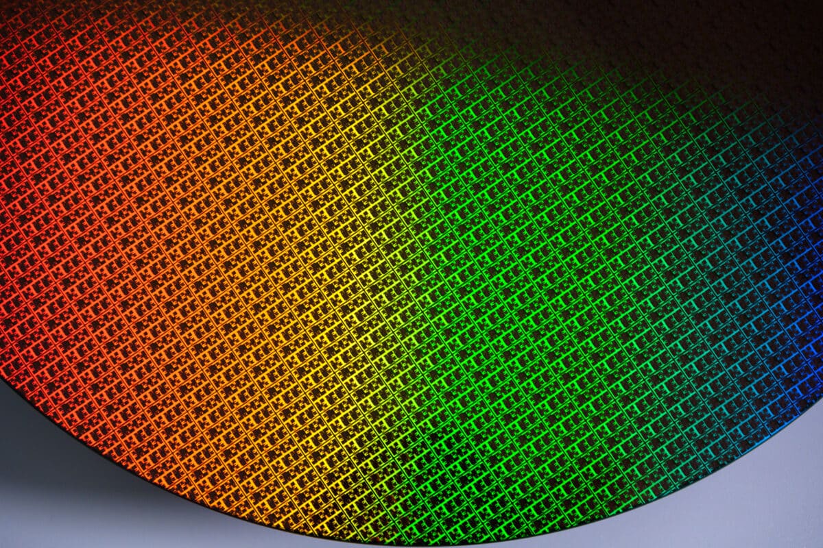
Intel Foundry has processed more than one million 300mm wafers using ASML’s High-NA EUV lithography, a total that includes equipment installation and qualification, research, development, and commercial manufacturing. The company already uses this technology on select layers of some Panther Lake processors built on Intel 18A, and it’s working with ASML on an even bigger shift: replacing today’s masks with a 6×12-inch format designed to remove some of the limitations High-NA introduces.
Key points on Intel’s million High-NA EUV wafers in 20 seconds
- Intel Foundry has now processed more than one million wafers using High-NA EUV.
- The figure includes testing, R&D, qualification, and commercial production, not one million finished chips.
- Some layers of certain Panther Lake chips built on Intel 18A already use this lithography.
- Current masks force large exposures to be split via stitching.
- Intel and ASML are preparing 6×12-inch masks to recover the full field and improve throughput.
The announcement coincides with the SPIE Photomask Technology + Extreme Ultraviolet Lithography conference, held this week in Monterey, California, where Intel Foundry and ASML are detailing how mature the new lithography generation has become.
The milestone carries an important message: High-NA EUV is ceasing to be purely an experimental technology.
Intel says overlay, throughput, and equipment availability are meeting its expectations, and that layers manufactured with High-NA on Intel 18A deliver results equal to or better than equivalent layers produced with conventional 0.33 numerical-aperture EUV machines.
But reaching one million wafers doesn’t mean Intel has manufactured one million complete processors using High-NA exclusively.
The company uses these machines only on selected layers of a portion of its Intel Core Ultra Series 3 chips, known as Panther Lake. The rest of the process combines other lithography techniques.
From 0.33 to 0.55 NA: why High-NA EUV matters so much
Conventional EUV (Extreme Ultraviolet) lithography currently uses a numerical aperture of 0.33 NA.
High-NA raises that figure to 0.55.
Numerical aperture determines, among other factors, the optical system’s ability to resolve extremely small structures. Increasing it allows finer features to be printed and reduces the need to rely on multiple exposures for certain layers.
That’s one of the reasons ASML views High-NA as a necessary technology for the next generations of advanced manufacturing.
Intel was also the first manufacturer to receive a commercial system of this kind.
ASML and Intel completed installation of the first commercial TWINSCAN EXE:5000 at Intel’s research facility in Hillsboro, Oregon, in 2024.
Progress since then has been rapid.
By late February 2025 Intel reported having processed roughly 30,000 wafers using High-NA EUV. It has now surpassed one million cumulative.
That jump reflects both increased utilization and the expansion and maturing of the infrastructure.
Intel has EXE:5000 systems and has also moved toward the EXE:5200B generation, designed to boost throughput compared with the first High-NA tools.
In July 2026 ASML also confirmed that Intel had qualified High-NA for certain Intel 18A product layers and that the technology was being used in high-volume manufacturing.
Panther Lake thus became the first high-volume logic product to incorporate High-NA EUV in part of its process.
The potential benefit goes beyond printing smaller structures.
If High-NA can replace several conventional EUV exposures with a single one, it can also reduce process steps, manufacturing time, and complexity.
Research on DRAM presented during 2026, for example, is looking precisely at moving from multipatterning schemes using 0.33 NA EUV to a single exposure using High-NA.
But the new optics bring an unexpected problem: the area that can be exposed at once is smaller.
The half-field problem and why Intel needs stitching
Conventional EUV machines use masks roughly six inches across and optics with 4X magnification in both directions.
This setup allows for a maximum field of about 26x33mm on the wafer.
High-NA changes the optics.
EXE systems use anamorphic magnification: roughly 4X in one direction and 8X in the other.
This is necessary to handle the angles that appear as numerical aperture increases, but it brings an important consequence.
With today’s masks, the available field shrinks to roughly 26×16.5mm.
For a small chip, that may not be a problem.
But large processors, especially CPUs, GPUs, and data-center accelerators, can exceed that half field.
Intel and ASML then use a technique called field stitching.
The design is split into two regions that are exposed separately and then have to be aligned with extreme precision on the wafer.
On paper it sounds simple.
In advanced manufacturing, it isn’t.
The structures on either side of the seam have to connect correctly. An extremely small error can affect metal lines, vias, or other circuit elements.
The chip’s design also has to account for where that seam will fall.
Intel is working with electronic design automation (EDA) companies so their process design kits let designers lay out chip blocks with this constraint in mind.
The company considers stitching a valid solution for using High-NA right now.
Still, there’s an added penalty: throughput.
6×12-inch masks could change High-NA EUV
The long-term fix Intel is pushing for is surprisingly physical: make the mask twice as long.
The industry has used roughly 6×6-inch square photomasks for decades.
Intel is proposing a move to 6×12 inches.
With a much larger usable surface, High-NA’s anamorphic optics could once again cover a full field of roughly 26x33mm without splitting it into two exposures.
That would make it possible to manufacture large chips without stitching and make better use of the machines’ throughput.
A paper presented at SPIE on large-format masks points to exactly two advantages: eliminating the field-stitching problem and boosting High-NA’s throughput, with the potential to cut costs.
However, changing the size of a mask format used by the entire industry for decades isn’t as simple as manufacturing a bigger rectangle.
Practically the entire photomask ecosystem would have to adapt.
Companies would need to modify or develop new mask blanks, deposition, etching, cleaning, and inspection systems, metrology tools, mask writers, protective films or pellicles, transport mechanisms, and handling equipment.
The scanners themselves will need to evolve to accept the new format.
Intel has spent more than three years working with ASML, mask makers, materials suppliers, EDA companies, and automation firms to prepare for that transition.
The initiative also runs on a long timeline.
ASML expects to demonstrate a pilot line based on larger masks around 2031 and bring the technology to high-volume manufacturing by around 2033, according to plans announced on September 8, 2026.
The company estimates the change could improve system throughput by roughly 40% compared with using a half field.
Intel gets there first, but TSMC and Samsung are also preparing High-NA
Intel currently holds a clear edge in accumulated experience with these machines.
It was High-NA’s first commercial customer, has spent years working with ASML, and already uses the technology on certain layers of a high-volume product.
That doesn’t mean its rivals have ruled out High-NA.
TSMC, Samsung, SK hynix, and other manufacturers are evaluating the technology, though their timelines differ.
Reuters notes that TSMC is considering introducing High-NA around 2030, while Samsung and SK hynix are targeting its use in DRAM around 2028.
TSMC’s strategy has traditionally been more conservative about introducing new tools before they deliver a sufficient economic advantage.
The cost isn’t small either.
The first High-NA systems run around $400 million per unit, according to estimates cited by Reuters. That forces manufacturers to justify adopting them through performance gains, fewer process steps, or the ability to manufacture features too complex for conventional EUV.
Intel is taking a different approach.
Its bet is to learn how to use High-NA ahead of its rivals, even while limitations like the half field still exist.
The million wafers accumulated matter for exactly that reason.
It isn’t just a production number. It means Intel has been able to gather data on resists, masks, defects, overlay, throughput, maintenance, and real-world equipment behavior at a scale other manufacturers haven’t yet reached in production.
One million wafers doesn’t mean High-NA has won yet
The figure also needs context.
Intel counts within that million the wafers used during installation, qualification, research, development, and commercial production.
So it shouldn’t be read as one million wafers going entirely toward processors sold on the market.
Nor does it mean High-NA will quickly replace conventional EUV.
Fabs will use both generations for years.
A 0.33 NA machine can still be economically preferable for layers where its resolution is sufficient. High-NA makes more sense where it avoids multiple exposures or where dimensions can no longer be resolved efficiently with the previous generation.
Advanced lithography is thus heading toward an increasingly heterogeneous infrastructure.
A single wafer can pass through DUV, conventional EUV, and High-NA EUV lithography depending on each layer’s needs.
For Intel, surpassing one million wafers shows that the latest of these technologies has already left the lab.
The next challenge is making it economically competitive at scale.
And that’s where the seemingly simple 6×12-inch masks could end up being almost as important as the hundred-million-dollar machines that use them.
Frequently Asked Questions
What has Intel achieved with High-NA EUV?
Intel Foundry says it has processed more than one million 300mm wafers using its High-NA EUV systems. The figure includes qualification, testing, R&D, and high-volume manufacturing of certain layers on some Panther Lake processors.
What’s the difference between EUV and High-NA EUV?
Conventional EUV uses a numerical aperture of 0.33, while High-NA raises that figure to 0.55. This improves resolution and can allow certain structures to be printed with fewer lithography steps.
Why does High-NA need stitching for large chips?
Its anamorphic optics shrink the field that can be exposed with current masks to roughly 26×16.5mm. Larger designs need to be split into two exposures and the two fields joined with high precision.
What are the future 6×12-inch masks for?
The format would restore roughly a full 26x33mm field with High-NA and eliminate stitching for many large chips. Adopting it requires modifying much of the photomask manufacturing and handling ecosystem.
This builds on Intel’s earlier rollout: see Intel debuts High-NA EUV at Panther Lake, pressures TSMC and Samsung and ASML looks beyond High-NA: Hyper-NA prepares the future of EUV for more on where this technology is headed.
