
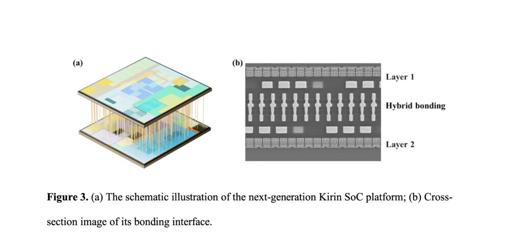
Huawei is using a new chip architecture called LogicFolding to boost compute density without relying solely on shrinking transistor size. The company says the technique can cut clock buffers by around 50% by shortening the chip’s internal connections, but an analysis from a semiconductor specialist points to a different limitation: when active silicon layers are stacked, heat dissipation can become a problem for reaching high frequencies in mobile processors.
Huawei’s LogicFolding: the key facts in 30 seconds
- LogicFolding reorganizes chip connections vertically and can combine different active silicon layers.
- Huawei says critical connections can be shortened by up to 70% and clock buffers cut by around 50%.
- The Kirin 9050 Pro in the new Mate 90 is Huawei’s first announced chip to use this architecture.
- The main technical debate now centers on heat dissipation as compute density increases.
- Qualcomm has clarified that its recent patent agreement with Huawei is not related to LogicFolding.
Huawei’s approach starts from a problem affecting the entire semiconductor industry: shrinking transistors is still useful, but each new manufacturing generation gets more complex and expensive. The company is also trying to gain performance through the chip’s architecture and internal interconnects.
LogicFolding is part of what Huawei calls the Tau (τ) scaling law, which it presented in May 2026. Rather than focusing solely on the geometric shrinking of transistors, this approach tries to reduce the time signals need to travel through the system. The company says LogicFolding makes it possible to shorten certain critical paths and lower the resistive and capacitive loads associated with connections.
The first announced commercial application has arrived with the Kirin 9050 family, used in the new Mate 90 phones. According to Huawei, the Kirin chips planned for fall 2026 would be the company’s first to incorporate LogicFolding. Reuters has also confirmed that the Kirin 9050 Pro uses this architecture, although Huawei hasn’t publicly detailed every element of the manufacturing process.
How LogicFolding Works and Why It Cuts Down Connections
The difference from a conventional design lies in how the circuits are physically arranged. Instead of keeping all the blocks mainly on a single plane, LogicFolding allows active silicon layers to be placed one on top of another and connected through very short vertical links.
Images of the Kirin 9050 Pro analyzed by Kurnal Insights show a compute die and an SRAM memory die joined through a hybrid copper-to-copper bonding process. The connection pitch sits at roughly 1.5 micrometers, according to the analysis cited by Wccftech.
The benefit being sought is straightforward: the shorter the distance certain signals have to travel, the lower the resistance and capacitance associated with those connections can be. Huawei says the typical length of internal interconnects can be reduced by around 20%, while some critical paths could be shortened by up to 70%.
That change has a knock-on effect on the clock distribution network. Modern processors need a clock network that distributes the synchronization signal across large areas of the chip, using numerous buffers to maintain signal integrity. If the distances are shorter, that network can be simplified.
Huawei says LogicFolding cuts the number of clock buffers by around 50%. Fewer buffers also mean less capacitance to charge and discharge on every cycle, which can reduce some of the power consumption tied to this infrastructure.
The company presents this architecture as a way to increase effective density and improve performance without requiring each silicon layer to achieve, on its own, the transistor density of a more advanced manufacturing node.
That’s an important distinction. The architecture doesn’t automatically turn a less advanced manufacturing process into a smaller one. What it tries to do is get more performance out of the available silicon through a different arrangement of circuits and connections.
Heat Introduces a Different Limitation
The main question is what happens when several active silicon layers concentrate power in a small space.
The semiconductor specialist identified on X as @Taog_1575 has compared the problem to some of the thermal difficulties associated with other advanced integration techniques, such as delivering power from the back side of the silicon, known as a Backside Power Delivery Network (BSPDN).
Their argument is that shortening connection lengths can reduce certain losses and local thermal density, but it doesn’t eliminate the problem of extracting the heat generated by the active layers. When silicon is stacked, some of the surfaces that traditionally help dissipate heat stop being directly exposed to the cooling system.
As a result, the limit may shift from the power consumption of the interconnects toward dissipation capacity. In a smartphone, this carries even more weight because the thermal margin is small and the cooling system is very different from what a server processor can use.
The specialist argues that this thermal limitation could affect the maximum frequency that proves practical with LogicFolding. They also claim that Qualcomm and Apple aren’t betting on this technology for their mobile processors precisely because of that problem. That last assessment should be treated as an independent expert’s opinion, not an official position from either company.
There’s also no public evidence allowing the conclusion that Apple has formally ruled out LogicFolding after evaluating the technology. Huawei, for its part, presents the architecture as one of the paths it intends to keep using to increase the performance of its chips.
The Qualcomm Deal Doesn’t Prove LogicFolding Has Been Adopted
The issue got more complicated this week with the announcement of a new patent agreement between Huawei and Qualcomm. Initially, several reports linked the deal to LogicFolding, but Qualcomm later clarified that connection is incorrect.
The agreement announced on October 5 includes cross-licenses on patent portfolios in areas such as 5G, computing, artificial intelligence and networking. It also includes Qualcomm’s purchase of certain U.S. Huawei patents related to computing, artificial intelligence, networking and other technologies.
Qualcomm has explicitly denied that the agreement is related to LogicFolding and has also rejected reports describing the company as a net payer in the deal. Therefore, the agreement can’t be used as proof that Qualcomm has adopted, licensed or will use Huawei’s chip architecture.
The confusion matters because a potential LogicFolding license would have been an important signal about a mobile processor maker’s interest in this technology. With Qualcomm’s clarification, that conclusion is no longer backed by the announced agreement.
Huawei has, however, managed to get its work on semiconductor architecture and its Tau scaling law to draw attention outside China, including earlier debates over whether 3D chip stacking can get around thermal limits. The company is trying to offset limited access to certain advanced manufacturing equipment through a combination of chip design, packaging, interconnects and new architectures.
Huawei itself says that over the past six years it has designed and produced 381 chips based on the principles of its Tau scaling law, and that its high-end designs could reach a transistor density equivalent to 1.4-nanometer processes by 2031. These are the company’s own targets and forecasts, not independent results that would make it possible to equate those designs today with the manufacturing processes of the industry’s leaders.
The LogicFolding case thus sums up one of the debates gaining weight in semiconductors. As shrinking the transistor gets harder, performance can also be pursued through how silicon is connected, stacked and organized. But increasing physical density doesn’t solve every problem on its own: power, frequency and, especially, heat removal still impose limits.
The Kirin 9050 Pro will show just how far Huawei’s architecture can turn those theoretical advantages into real improvements in a commercial device. For now, the public data supports talking about a new design strategy and Huawei’s claims about its benefits, but not yet an independent demonstration that LogicFolding can compete in every scenario with the advantages gained through more advanced manufacturing nodes.
Frequently asked questions
What is Huawei’s LogicFolding?
LogicFolding is an architecture that reorganizes part of the circuits and their connections across several silicon layers, using short vertical links. Huawei includes it in its Tau scaling strategy to reduce signal propagation times.
What improvement does Huawei promise with LogicFolding?
Huawei says typical connections can be shortened by around 20%, some critical paths by up to 70%, and clock buffers by roughly 50%.
What is LogicFolding’s main problem?
The main technical question concerns heat dissipation when several active silicon layers are placed very close together. A specialist cited in analyses of the technology believes this limitation could affect the frequencies that end up being viable in mobile chips.
Has Qualcomm bought LogicFolding technology from Huawei?
Qualcomm has clarified that its recent patent agreement with Huawei is not related to LogicFolding. The agreement does include cross-licenses in 5G, computing, artificial intelligence and networking, along with the purchase of certain U.S. Huawei patents.
