
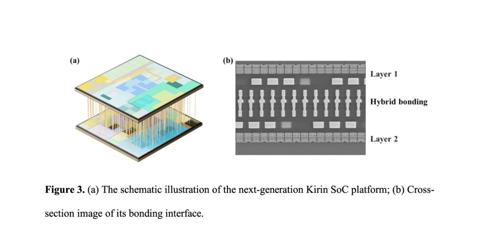
Huawei wants to show that stacking logic in three dimensions doesn’t have to turn a processor into a thermal problem. The company has published new data on its Kirin 2026, the first mobile SoC to use its LogicFolding architecture under the so-called Tau (τ) Scaling Law, which it says has boosted transistor density by around 55% while cutting power consumption in several parts of the chip at equal performance. The proposal aims to move beyond classic scaling based solely on making transistors smaller and smaller.
Huawei Kirin 2026 key facts in 20 seconds
- Huawei claims LogicFolding boosts the Kirin 2026’s density by about 55% versus the Kirin 9030 Pro.
- The architecture splits logic across active layers connected vertically through hybrid bonding.
- At equal performance, the company reports power cuts of 66% in the NPU, 58% in the GPU, and 41% in the high-performance CPU core.
- The main challenge remains controlling heat, alignment, manufacturing yield, and EDA tools.
The approach was publicly presented by Huawei during 2026 and later expanded in a second version of the paper A time scaling theory for multi-layer electronic systems, published on ChinaXiv. It’s a preprint, so the results reported by the company still don’t amount to independent validation or tests on commercial devices carried out by outside labs.
That caution is especially necessary because Huawei presents Tau Scaling as something broader than a new packaging technique. The idea is to change the yardstick for improvement: instead of measuring progress solely by how much a transistor can be physically shrunk, try to cut the time information needs to travel through the device, the circuits, the chip, and the system.
LogicFolding: Shortening Wires Instead of Always Shrinking the Transistor
The most visible implementation of that theory is LogicFolding.
Three-dimensional chips aren’t new, and this isn’t Huawei’s first attempt at 3D stacking to bypass process-node limits. The industry has used stacking in memory like HBM for years and is developing increasingly sophisticated technologies to fit multiple dies inside the same package. What’s less common is stacking large amounts of active logic, because CPUs, GPUs, or NPUs generate far more heat than a memory layer.
Huawei proposes splitting digital, analog, and memory circuits across different active layers and connecting them through extremely dense vertical links.
According to the published data, the Kirin 2026 uses a 1.5-micron hybrid bonding pitch and around 50 million vertical interconnects. Between 10% and 15% of these are dedicated to signal transport. Huawei also says the Kirin 2027’s test silicon has already narrowed that pitch to 1 micron and surpasses 100 million vertical connections.
The goal isn’t simply to pack twice as much silicon into the same projected surface area.
By splitting a circuit across two layers, a connection that previously ran a relatively long horizontal distance can become a much shorter vertical link. Huawei says LogicFolding cuts typical interconnect lengths by about 20%, and that certain critical paths can be shortened by up to 70%.
That matters because moving information also consumes energy.
The longer a metal line is, the higher its resistance and parasitic capacitance can be. Charging and discharging those interconnects millions or billions of times per second accounts for a significant share of a modern processor’s power budget.
Tau Scaling tries to recover that energy by reducing the distances traveled.
The Kirin 2026 Tests the Big Objection: Heat
The major difficulty appears immediately once another active layer is added.
If more logic is packed into the same space and one layer ends up physically farther from the heatsink, you’d expect higher thermal density and temperatures that are harder to control.
That’s precisely the objection Huawei is trying to answer with its new data.
According to the measurements the company disclosed, the Kirin 2026’s transistor density goes from the Kirin 9030 Pro’s 155 million transistors per mm² to 238 million per mm², around 53-55% higher depending on the calculation method used.
But Huawei argues that this increase doesn’t necessarily come with higher power consumption.
In a comparison of the high-performance CPU core at equal performance, voltage reportedly dropped from 1.1V to 0.9V, while normalized power consumption falls 41%. At the same time, normalized area shrinks 37.5%, meaning the resulting power density would be roughly 5.6% lower.
Data disclosed in September extends that comparison to other blocks.
Huawei reports 66% lower power consumption in the NPU, 58% lower in the GPU, and 41% lower in the high-performance CPU core when compared at the same performance level. For the NPU, the company says it kept 29 TOPS while significantly reducing frequency and voltage, with a 73% drop in power density.
These are striking figures, but they should be understood as Huawei’s own results under selected iso-performance scenarios.
Tau doesn’t automatically turn 3D integration into a low-power technology.
Huawei’s own explanation acknowledges that this is a time-scaling law, not an energy-scaling one. If the margin gained from shortening the paths is used to raise clock speeds instead of lowering voltages, power consumption and temperature can climb right back up.
Thermal Design Becomes Part of the Architecture
LogicFolding also forces the processor to be designed from the start around where heat is generated.
Huawei describes a thermal-aware floorplanning approach, in which the different units are distributed across layers after studying their thermal maps. The highest-consumption blocks shouldn’t be placed directly on top of one another if that configuration creates hotspots that are hard to dissipate.
This detail matters because it shows that the answer to the thermal problem doesn’t depend solely on a better cooling material.
It’s a combination of architecture, voltage, physical layout, vertical connectivity, and packaging.
For future generations with more layers, Huawei is proposing even more aggressive solutions. The documentation tied to Tau Scaling V2 mentions heat-spreading layers made of chemical-vapor-deposited (CVD) diamond and internal microchannels for fluorinated liquid cooling. The theoretical goal would be managing power densities of up to 300 W/cm² in configurations aimed at AI chips.
Those technologies are part of the roadmap and shouldn’t be confused with confirmed commercial features of the Kirin 2026.
Huawei Is Looking to Gain Density Without Relying Solely on Advanced Lithography
The industrial backdrop also explains the appeal of the proposal.
Huawei faces restrictions on access to certain Western semiconductor manufacturing technologies and can’t rely as easily as other designers on TSMC’s most advanced nodes.
LogicFolding lets Huawei try to claw back some of that disadvantage by shifting the competitive edge from the transistor toward architecture and 3D integration.
Futurum Group points out that the 1.5-micron pitch Huawei has disclosed would be a significant technical claim if it can be sustained at scale, though Intel and TSMC still hold an edge in advanced processes and are also developing their own hybrid bonding technologies.
That rules out reading Tau Scaling as a simple substitute for lithography.
Huawei isn’t necessarily proposing to abandon geometric shrinking either. The strategy consists of combining available process improvements with shorter distances, vertical integration, and a redesign of how data moves.
What remains to be proven is whether the method can be manufactured with good yields, competitive costs, and sufficient uniformity.
Wafer-to-wafer integration adds its own problems: wafer warpage, alignment precision, bonding defects, and the loss of good chips when one of the layers has a fault.
Huawei acknowledges there are still challenges around bonding pitch, warpage, overlay precision, and adapting electronic design automation (EDA) tools, with work expected to continue over the next three to five years.
From Kirin to Ascend: The Bet Doesn’t End With Phones
Huawei sees the Kirin 2026 as an initial application of a much broader strategy.
The V2 version of Tau Scaling also places LogicFolding integration in future generations of Ascend AI processors. TrendForce notes that the roadmap envisions introducing this architecture around 2030 and moving toward configurations with three or more active layers.
The plan also calls for gradually lowering the hybrid bonding pitch below 1 micron and surpassing 200 million vertical connections.
On paper, that would bring interlayer interconnect density close to the density of the chip’s own internal wiring. Layers would then stop behaving like relatively independent dies and could be designed almost as a single three-dimensional logic structure.
That’s probably the most interesting aspect of Tau Scaling.
Huawei isn’t just claiming it can stack chips. The industry already knows how to do that.
Its bet is to make the bond between two layers dense enough that the vertical dimension becomes an ordinary part of circuit routing.
The Kirin 2026 will be an early test of how far that idea can go.
The density and power figures Huawei has published look promising, but essential pieces are still missing: independent testing, sustained thermal performance inside an actual phone, manufacturing yields, costs, and comparison against commercial processors built on more advanced nodes.
If that data ends up backing the initial claims, LogicFolding could demonstrate that the future of scaling doesn’t depend solely on shrinking nanometers.
It could also mean traveling less distance.
Frequently Asked Questions
What is Huawei’s Tau Scaling Law?
It’s a scaling proposal that uses the time and latency of information movement as its optimization benchmark, rather than relying exclusively on shrinking the physical size of transistors.
What is LogicFolding?
It’s a 3D integration architecture that distributes parts of the same circuit across different active layers and connects them through high-density hybrid bonding to shorten signal paths.
Does the Kirin 2026 use less power even though it has more transistors per mm²?
Huawei says yes, in certain tests at equal performance. The company reports roughly 55% higher density along with power cuts of 41% in the CPU, 58% in the GPU, and 66% in the NPU. These are the manufacturer’s own results and still require independent validation.
Has Huawei definitively solved the thermal problem of 3D chips?
No. The initial results indicate that lowering voltage and shortening distances can offset part of the density increase, but challenges around cooling, manufacturing, alignment, EDA, and scaling to more layers still remain.
