Huawei re-emerges at the center of the semiconductor race with an ambitious rumor: the future Kirin 9050, presumably destined for a next-generation of Mate phones, could use 3D stacking technology to enhance performance and density without relying on the most advanced nodes from TSMC or Samsung. Some leaks even suggest that the chip has outperformed the Apple A18 Pro in internal tests, although benchmarks, power consumption, and conditions of those supposed measurements are not yet known.
That nuance is important. There is no official technical specification for the Kirin 9050; Huawei has not publicly confirmed the chip’s performance, and comparisons with Apple should be viewed as unverified information. Still, the rumor aligns with a strategy that is much better documented: Huawei is trying to compensate for the limitations imposed by U.S. sanctions through design, packaging, architecture, and system integration—not just transistor size reduction.
The Chinese company recently presented its Tau Scaling Law approach and LogicFolding architecture, a line of research aiming to continue increasing the actual performance and density of chips even though China does not have full access to the most advanced EUV lithography. According to Reuters, Huawei aims to reach densities equivalent to 1.4 nm by 2031 through architectural and system optimization, while the country still lags in advanced manufacturing compared to TSMC, Samsung, and Intel.
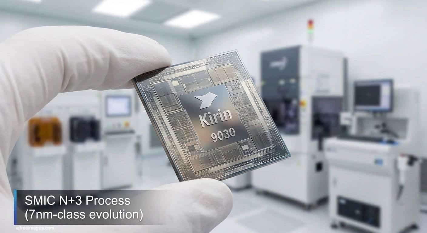
The rumor of the Kirin 9050 and 3D stacking
Published information indicates that the Kirin 9050 could employ a 3D IC stacking solution, meaning vertical stacking of components within the chip or package. The idea is to increase density and reduce internal distances without fabricating everything on an extreme node like 3 nm or 2 nm. In practice, performance depends not only on the transistors but also on how blocks are connected, how long data takes to move, and how much energy is lost along those paths.
This is precisely where Huawei appears to be concentrating its efforts. If SMIC cannot produce at scale with EUV and struggles to match TSMC’s leading nodes, the alternative is to push DUV processes, improve design, adopt more advanced packaging techniques, and reorganize chip logic. It’s not a straightforward path, nor does it eliminate the advantage held by global leaders; however, it can help close the gap on certain products.
| Element | Current Situation |
|---|---|
| Kirin 9050 | Unconfirmed rumor from Huawei |
| Performance vs. A18 Pro | Supposed leak, no benchmarks or power data published |
| Technology mentioned | 3D stacking and possible use of LogicFolding |
| Manufacturing | Likely linked to SMIC, but no official data |
| Underlying challenge | Lack of access to advanced EUV in China |
| Huawei’s strategy | Improve performance through architecture, packaging, and system integration |
The comparison with Apple is striking because the A18 Pro is a chip manufactured by TSMC using second-generation 3 nm technology, designed for efficiency, advanced graphics, and Apple Intelligence. Apple highlighted a new CPU, a six-core GPU, and a 16-core Neural Engine that are faster and more efficient. Huawei, on the other hand, would need to offset manufacturing disadvantages with system design.
Why “exceeds the A18 Pro” isn’t enough on its own
The headline claiming that a Kirin 9050 could surpass the A18 Pro sounds impressive, but it says little technically unless the specific test is explained. A mobile chip can excel in multi-core CPU performance and still consume more power. It can temporarily outperform in GPU benchmarks but then fall short due to temperature. It might deliver good AI results but require more energy. It could perform well in a lab prototype but not within a phone with limited battery, cooling, and thermal management.
Therefore, any serious comparison should include at least four data points: the benchmark used, operating frequency, sustained power consumption, and real device performance. Without this information, the rumor helps understand Huawei’s technological direction but cannot assert that the Kirin 9050 is objectively superior to the A18 Pro.
| Comparison | Apple A18 Pro | Kirin 9050, according to rumors |
|---|---|---|
| Status | Confirmed commercial product | |
| Manufacturing | TSMC 3 nm second-generation | |
| Approach | High-performance mobile and Apple Intelligence | |
| Public data | CPU, GPU, Neural Engine details provided by Apple | |
| Performance comparison | Based on commercial data and external tests | |
| Main unknown | Runtime, temperature, sustained performance, yield |
This is especially critical for mobile devices. A SoC doesn’t operate in an ideal test environment but inside a thin device with limited battery, camera, modem, display, and strict thermal constraints. If Huawei increases density through stacking, it must also manage heat, interconnects, fabrication challenges, reliability, and sustained performance.
Huawei is trying to change scaling rules
The most interesting aspect isn’t whether the Kirin 9050 beats a specific Apple benchmark. What matters is that Huawei is attempting to redefine how it competes when it cannot access the same manufacturing equipment as its rivals.
The Tau Scaling Law approach suggests focusing less on traditional geometric scaling and more on signal propagation time. Simply put, it’s about making data travel shorter distances, arrive faster, and consume less energy. LogicFolding, as explained publicly by Huawei, aims to reorganize logic to reduce delays and increase effective density.
These ideas are not exclusive to Huawei. The entire industry is exploring chiplets, advanced packaging, 3D stacking, proximity memory, and heterogeneous architectures because classical Moore’s Law scaling is no longer making leaps at the same cost. For Huawei and China, this transition is not only technical but also geopolitical.
For years, the U.S. has limited Huawei and other Chinese players’ access to critical technologies. SMIC has managed to produce advanced chips with DUV and complex techniques, but Reuters and other sources note that China remains several generations behind leading manufacturing. This situation compels seeking architectural shortcuts.
What it could mean for the mobile industry
If the Kirin 9050 demonstrates some of these improvements in a commercial product, Huawei could strengthen its position in the high-end Chinese market and further reduce dependency on foreign chips. It would also send a political and technological message: even without EUV, China can find ways to stay competitive in certain segments.
However, it’s important not to overstate this. Surpassing the A18 Pro, if confirmed, wouldn’t automatically elevate Huawei above Apple or TSMC. Apple continues progressing with new chip generations, and TSMC is moving towards 2 nm and beyond. Additionally, chip performance depends not only on the SoC but also on the operating system, memory, modem, energy efficiency, software, compilers, app ecosystems, and overall user experience.
Huawei’s evolution deserves attention because it illustrates how sanctions have reshaped Chinese innovation. Instead of halting development entirely, they have prompted Huawei to invest in proprietary design, packaging, AI accelerators for Ascend, mobile Kirins, and new scaling strategies. The company is turning industrial limitations into architectural challenges.
The Kirin 9050 could be a real breakthrough, a partial improvement, or just an inflated rumor. What is clear is that Huawei is not simply waiting for the same access to ASML as its competitors. It is seeking performance through alternative routes.
The mobile chip race is no longer just about nanometers. It’s about packaging, power consumption, memory, interconnects, software, and turning restrictions into innovative architecture. Huawei aims to prove that it still has room to surprise us.
Frequently Asked Questions
Has Huawei officially confirmed the Kirin 9050?
No. The available information about the Kirin 9050 and its supposed performance against the A18 Pro comes from rumors and leaks, not from an official launch.
Can a chip fabricated on a less advanced node outperform a 3 nm chip?
It can happen in specific tests if design, architecture, memory, or packaging compensate for some disadvantages. But power consumption, temperature, and sustained performance are also critical factors.
What is 3D stacking in chips?
It’s a technique that vertically stacks components or silicon layers to increase density, reduce internal distances, and improve communication between blocks.
What is LogicFolding?
It’s an architecture introduced by Huawei as part of its Tau Scaling Law approach, aimed at improving performance and effective density by reducing signal delays and reorganizing logic.