
The Institute of Microelectronics at the Chinese Academy of Sciences (CAS) has developed a gate-all-around (GAA) transistor architecture built using a process based on deep ultraviolet (DUV) lithography. The institute says the integration it achieved exceeds an on/off current ratio of 5 × 10⁵, opening an experimental path toward performance associated with 3nm-class nodes without relying on EUV lithography as the core technology.
China’s DUV-based GAA transistors in 30 seconds
- The Chinese Academy of Sciences has completed a preliminary integration of GAA with stacked nanosheet channels, built using DUV.
- The transistor reaches an Ion/Ioff ratio above 500,000, according to data reported by the Institute of Microelectronics.
- The architecture improves the transistor’s electrical control and allows some easing of the requirements on FEOL structure pitch.
- The bottleneck shows up in MEOL and M0 interconnects: the full design doesn’t automatically add up to a 3nm node.
- A technical analysis places a possible configuration at around 137.8 million transistors/mm², comparable to 5nm-class densities.
The development comes from a presentation given on September 16 in Beijing by Ye Tianchun, director of the Chinese Academy of Sciences’ Institute of Microelectronics and one of the technical leads on a national research program. According to reporting from DIGITIMES, the institute has laid out a development path for GAA devices for sub-3nm processes that doesn’t rely on extreme ultraviolet (EUV) lithography as its core technology.
What makes the research significant is that it separates two problems that usually come up together when discussing advanced nodes: the transistor itself, and the structures that connect it to the rest of the chip. China faces restrictions on access to certain advanced semiconductor manufacturing technologies and equipment. The United States maintains controls on manufacturing equipment, software, and other technologies tied to producing advanced chips in China.
That makes any advance capable of reducing reliance on EUV industrially significant. But the CAS’s work doesn’t mean China has managed to manufacture a complete 3nm chip using DUV. That distinction matters.
GAA improves the transistor, but doesn’t solve the whole chip
GAA transistors represent an evolution beyond FinFETs. In a FinFET, the gate controls the channel from several sides around a vertical fin structure. In a nanosheet GAA, the gate fully surrounds each channel, increasing control over current flow.
That control becomes especially useful as physical dimensions shrink. One of the challenges with ever-smaller transistors is maintaining a large enough gap between the on state and the off state. The Ion/Ioff ratio is precisely what describes that gap.
The figure reported by the Institute of Microelectronics, above 5 × 10⁵, is equivalent to a difference of more than 500,000 times between on-state and off-state current under the measurement conditions used. DIGITIMES reports that the result comes from a process integration optimized for a GAA structure with stacked nanosheet channels.
The CAS had already worked on this type of architecture. In 2025, the Institute of Microelectronics itself published progress on nanosheet GAA and a surface treatment designed to reduce defects in the channels after releasing the silicon layers. At the time, the institute described GAA as one of the relevant structures for the evolution of logic processes below 3nm.
The new research adds another piece: the possibility of building this architecture within a manufacturing path that relies on DUV.
The bottleneck shifts from the transistor to the interconnects
The most interesting question comes up when looking at what happens after the transistor is built. An integrated circuit isn’t made up of transistors alone. They need to be wired together through a complex network of contacts, vias, and metal layers.
That’s where concepts like FEOL (Front-End-Of-Line), MEOL (Middle-End-Of-Line), and BEOL (Back-End-Of-Line) come in. FEOL mainly covers the manufacturing of the devices themselves. MEOL connects those devices to the first metal structures, while BEOL contains the upper interconnect layers.
The analysis published based on the CAS’s work notes that GAA’s strong electrical behavior may allow some relaxation of fin pitch — the spacing between the transistor’s active structures. That can free up space in logic cell design.
However, MEOL constraints remain in place. The contacts and the first metal layer, known as M0, still impose geometric conditions that the new transistor doesn’t eliminate on its own.
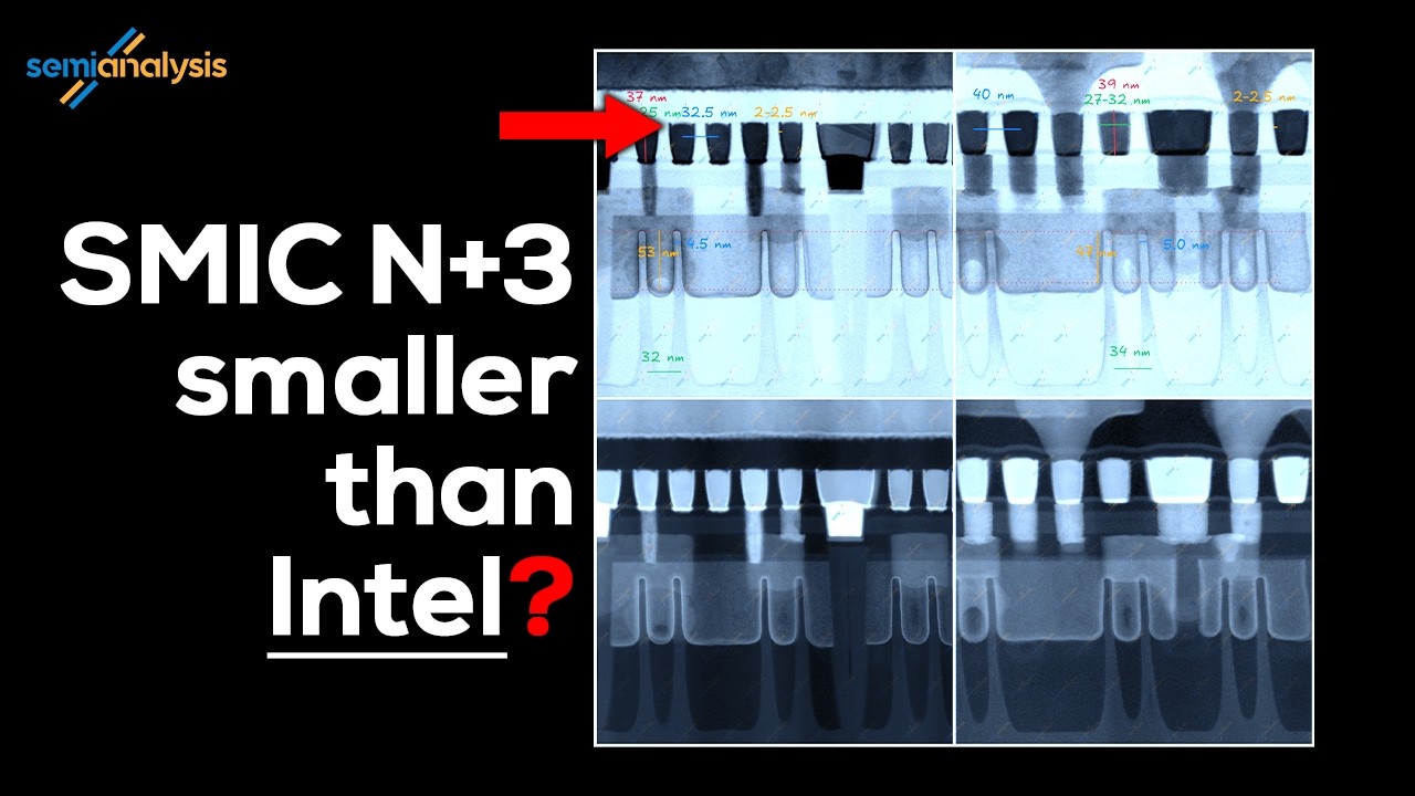
A technical analysis published by SemiAnalysis lays out exactly this scenario for a possible evolution of SMIC’s processes — building on earlier microscopic analysis of SMIC’s N+3 process used in Huawei’s Kirin 9030. In its estimate, a configuration with a 198nm cell height and a 54nm contacted gate pitch could reach a theoretical density of around 137.8 million transistors per square millimeter, in the density class associated with TSMC N5. The analysis itself stresses that this is a theoretical path, and that accumulating manufacturing difficulties could narrow the process margin.
That difference explains why a claimed path to 3nm needs to be read carefully. The transistor may offer electrical characteristics comparable to what’s needed at far more advanced nodes, but that doesn’t automatically turn the full process into a 3nm node.
The practical target described in the analysis is closer to 5nm-class density, achieved through a combination of GAA, reduced cell height, and a tighter configuration of the first metal layers. Moving from five to four tracks at M0 is one of the elements used in that estimate.
DUV, multi-patterning, and the limits of node naming
DUV lithography doesn’t have the direct optical resolution needed to draw all the structures of the most advanced nodes in a single exposure. The industry can compensate for this with multi-patterning techniques, where the same geometry is built through several stages of exposure, deposition, and etching.
The difficulty is that each additional step adds process complexity and can affect cost, manufacturing yield, and available margin. So reaching a given theoretical density with DUV doesn’t necessarily mean reproducing the same production conditions as a fab that uses EUV.
On top of that, node names stopped representing a single physical transistor dimension a long time ago. A process called “3nm” doesn’t mean every one of its structures measures 3nm. A proper comparison requires looking at density, yield, power consumption, pitch, interconnects, and other process characteristics.
The Chinese research is interesting precisely because it tries to change that equation. Instead of relying solely on shrinking printed dimensions, it uses a transistor architecture with greater electrical control to claw back margin elsewhere in the design.
The United States, for its part, has kept controls in place on technologies and equipment used to manufacture advanced semiconductors in China. In December 2024, the U.S. Department of Commerce added new restrictions on manufacturing equipment, software tools, and other elements tied to advanced processes. In 2025, it also tightened conditions applying to certain foreign-owned fabs operating in China.
The CAS research needs to be understood within that technological backdrop, but the reported result on its own doesn’t prove China has solved every industrial limitation tied to manufacturing 3nm chips.
It also remains to be seen how this architecture would evolve from an experimental device into a process technology with enough yield, uniformity, and volume for commercial production. There’s an important difference between demonstrating that a structure works and having a competitive manufacturing platform.
For the AI industry, the story also has an indirect angle. AI accelerators need increasing numbers of transistors, memory, and internal connections, and manufacturing restrictions can affect the ability to develop new processors. A path that raises density without relying on EUV could widen the design options available to Chinese chipmakers, though there isn’t yet enough public evidence to quantify which commercial products might benefit from this research.
FAQ
What has the Chinese Academy of Sciences developed?
The CAS’s Institute of Microelectronics has developed a preliminary integration of GAA transistors with stacked nanosheet channels using a DUV lithography-based path. The institute reported an Ion/Ioff ratio above 5 × 10⁵.
Does this mean China already manufactures 3nm chips with DUV?
No. The result demonstrates a transistor architecture and an experimental technology path, but it isn’t the same as commercial production of a complete 3nm chip. MEOL and M0 interconnects still impose limitations.
What density could this technology reach?
A technical estimate places a possible configuration at around 137.8 million transistors per square millimeter, a 5nm-class density. That’s a process estimate, not a commercial product specification.
Why does it matter to use DUV instead of EUV?
DUV is an older manufacturing technology that can be combined with techniques like multi-patterning to produce advanced structures. A GAA architecture that eases some geometric requirements can help extract more performance from that infrastructure, though the limitations of interconnects and large-scale manufacturing remain.
