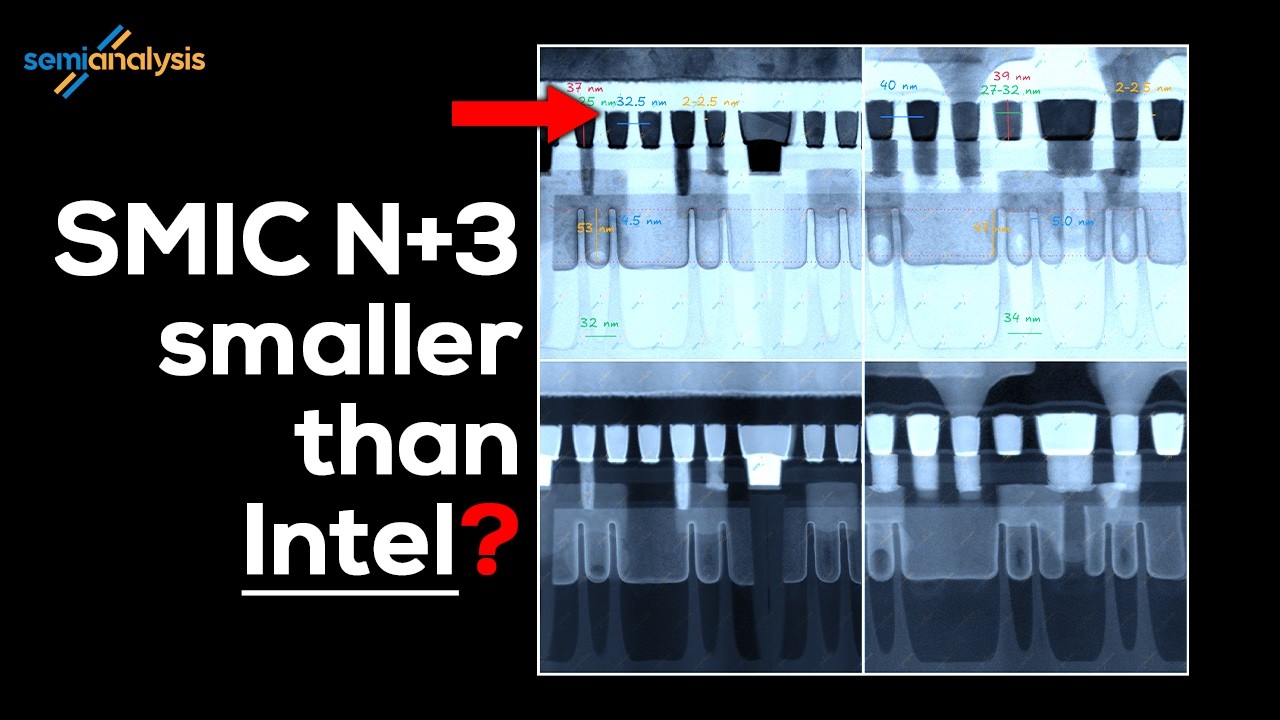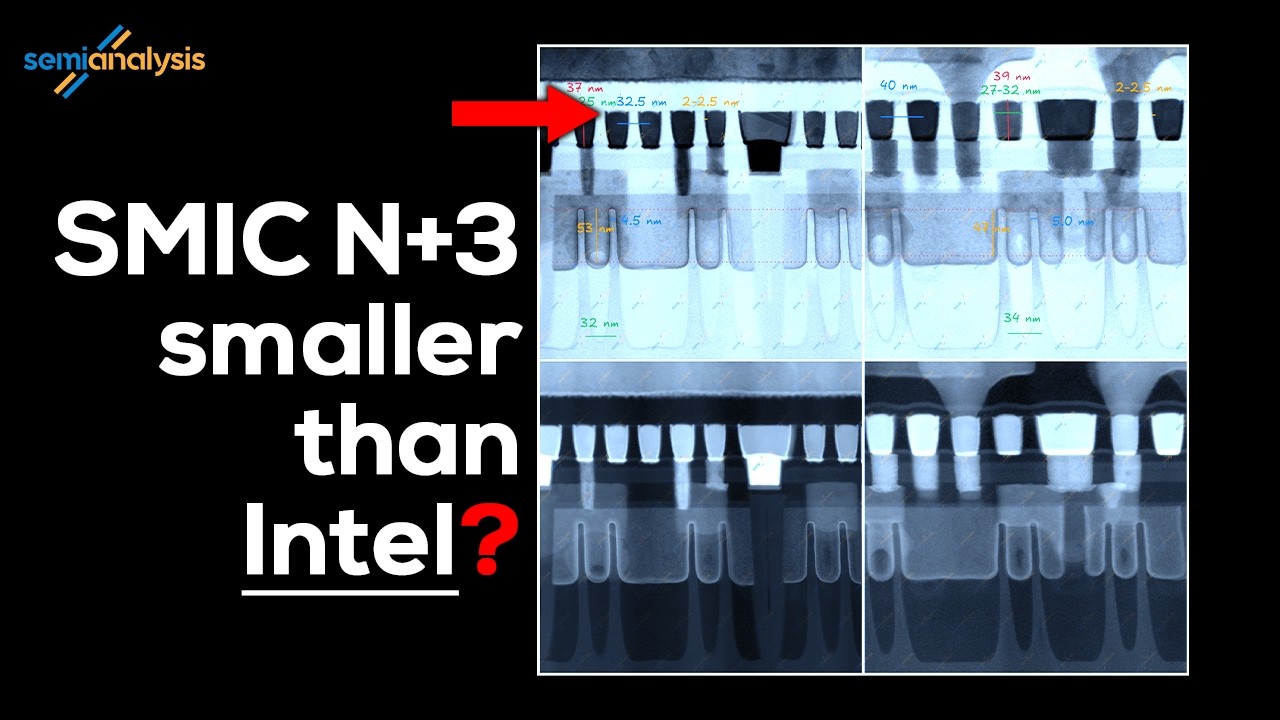
Microscopic analysis of Huawei’s Kirin 9030 has revealed an unexpected detail: SMIC’s N+3 process achieves a minimum metal step of 32.5 nanometers, compared to the 36 nanometers observed in Panther Lake chips manufactured with Intel 18A. This indicates how far China has reached without access to extreme ultraviolet lithography, but it doesn’t make the Chinese node more advanced than Intel’s.
The key points of the Kirin 9030 and SMIC N+3 process in 30 seconds
- SMIC has achieved a M0 step of 32.5 nanometers using DUV lithography and quadruple patterning.
- Panther Lake uses 36 nanometers, although Intel 18A supports designs at 32 nanometers.
- N+3 reaches 113.4 million transistors per mm², slightly more than TSMC N6.
- Intel 18A maintains higher logical density, better efficiency, and more advanced transistor and power technologies.
This finding comes from the first public report by SemiAnalysis’s STEEL lab, which physically opened the system-on-chip (SoC) of a Huawei Mate 80 and examined its transistors, interconnections, memory, and packaging via electron microscopy. The analysis confirms that the Kirin 9030 uses SMIC’s third-generation 7-nanometer process, known as N+3.
The comparison made headlines because a specific dimension of the Chinese chip is smaller than that observed in a product made with Intel 18A, a node several generations ahead on paper. However, using this single number to classify the entire process can be misleading.
A smaller metal step doesn’t mean a better node
The metal step measures the distance between interconnection lines within the chip. In this context, it refers to M0, one of the lower layers connecting elements inside logic cells.
SemiAnalysis measured an M0 step of 32.5 nanometers in the Kirin 9030, which is 19% smaller than SMIC N+2 and TSMC N6. In Panther Lake, the observed step was 36 nanometers. This suggests that this specific layer in Huawei’s chip is more compressed than the layer used in Intel’s commercial product.
However, Intel 18A supports an M0 step of 32 nanometers. Panther Lake mainly uses high-performance libraries with slightly wider cells and connections to favor speed, power, and manufacturability. The company didn’t need to utilize the densest configuration across all processor areas.
| Feature | SMIC N+3 in Kirin 9030 | Intel 18A in Panther Lake |
|---|---|---|
| Observed metal step (M0) | 32.5 nm | 36 nm |
| Node-supported M0 step | 32.5 nm | 32 nm |
| Transistor architecture | FinFET | RibbonFET, GAA type |
| Backside power delivery | No | Yes, PowerVia |
| Manufacturing techniques | DUV and SAQP | Advanced processes and PowerVia |
| Normalized logic density | 113.4 MTr/mm² | Approximately 61% higher in HD library |
The last row illustrates why metal step size isn’t synonymous with overall density. SemiAnalysis calculates N+3’s density at 113.4 million transistors per mm², versus 107.7 million in TSMC N6. Although noteworthy for a non-EUV fab, it’s about 38% below Intel 18A’s high-density library.
Density also depends on gate length, cell height, upper layers, line resistance, vias, SRAM memory, and routability. A narrow M0 layer saves local space but may impose constraints elsewhere in the design.
Additionally, Intel incorporates two technologies that SMIC hasn’t yet adopted in N+3. RibbonFET replaces FinFET transistors with gate-all-around (GAA) structures to improve channel control. PowerVia shifts power distribution to the wafer’s backside, freeing space on the front layers and reducing competition between power lines and signals. Intel attributes these innovations to enhanced density, frequency, and power efficiency.
How SMIC achieved 32.5 nanometers without EUV
SMIC has compensated for equipment limitations using deep ultraviolet (DUV) lithography, multiple patterning, and tight coordination between design and manufacturing.
The main technique identified for M0 is quadruple self-aligned patterning (SAQP). The manufacturer first prints an initial pattern, creates spacers along its edges, and repeats the process to split it into four narrower lines. This enables fabrication of features that conventional DUV exposure couldn’t directly resolve.
This approach requires more masks, depositions, etches, and alignments, each adding time, cost, and potential defect opportunities. Slight deviations in patterning can alter line widths or disrupt connections.
SMIC also leverages co-optimization of design and technology (DTCO). The Kirin 9030 uses cells with fewer fins per transistor, contact placement above the active gate, and tighter cell spacing—decisions that maximize surface but limit margins for performance, power, and manufacturability balance.
This process enables Huawei to increase resources for the Kirin without significantly enlarging the silicon die. SemiAnalysis estimates an area near 140 mm², which includes an additional intermediate core, more cache, and larger GPU and neural processing units compared to Kirin 9020.
This area efficiency is one of the key achievements of N+3. However, improvements in power and performance don’t scale proportionally.
Differences in power consumption and frequency
SemiAnalysis compares the main core of Kirin 9030 to roughly the performance-per-cycle of an Arm Cortex-X2, introduced in 2021. While it’s an advancement over previous Huawei chips, it still lags behind current Apple, Qualcomm, and MediaTek designs.
The least efficient comparison is Huawei’s main core versus Apple’s efficiency core. According to SemiAnalysis data, Apple’s small core delivers about 20% more performance at roughly 1 watt, while Kirin’s main core consumes about 4.5 watts. These are different architectures and not direct process comparisons, but they illustrate the energy gap.
Kirin also can’t reach the same voltage-frequency curves as chips made with recent TSMC or Intel nodes. A more efficient process allows higher frequency at lower voltage, or the same frequency with reduced power, freeing transistors for cache and execution/prediction units.
Therefore, the claim that SMIC surpasses Intel 18A needs clarification. SMIC has achieved a slightly more compact metal layer than Panther Lake but at the expense of a more complex process. Intel maintains a higher overall logical density, backside power delivery, and gate-all-around transistors.
Moreover, Panther Lake is a chiplet-based design, using Intel 18A for its compute tile, with other modules potentially coming from different processes and fabs. Intel began 18A production in 2025, with future enhancements like 18A-P promising about 9% more performance at the same power or 18% less power with equivalent performance.
The Chinese advancement still has industrial implications. Restrictions haven’t halted domestic chip development but have pushed SMIC and Huawei to focus more on DUV patterning, physical design, packaging, and system optimization.
Huawei is also exploring stacking technologies called LogicFolding, which layer active logic chips vertically. This could increase surface density and shorten interconnections, but it doesn’t match the efficiency of individual transistors in the most advanced nodes. The analyzed Kirin 9030 doesn’t yet employ this system.
SMIC remains behind Intel, TSMC, and Samsung in the metrics defining advanced nodes. Still, the Kirin 9030 shows that it’s possible to produce capable processors for phones, networks, inference, and other systems prioritizing supply independence.
Frequently Asked Questions
Is SMIC’s process more advanced than Intel 18A?
No. The Kirin 9030 uses a smaller M0 step than Panther Lake, but Intel 18A provides higher logic density, better electrical characteristics, and more recent technologies.
What density does SMIC N+3 achieve?
SemiAnalysis estimates 113.4 million transistors per square millimeter, slightly above TSMC N6 and about 38% below Intel 18A’s high-density library.
How does SMIC manufacture advanced chips without EUV?
By using DUV lithography with multiple patterning steps, including quadruple self-aligned patterning, and employing DTCO techniques to compact cells and connections.
Why does the Kirin 9030 consume more energy?
The N+3 process and Huawei’s architectures have less favorable voltage-frequency curves. To meet performance targets, they require more power than chips in recent nodes.