
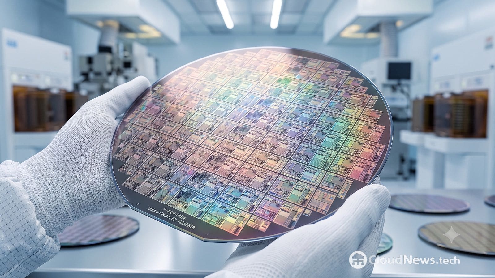
Applied Materials and Intel have expanded their collaboration to develop semiconductor manufacturing technologies for the next generations of artificial intelligence (AI) chips. The agreement, announced on October 6, 2026, focuses on improving transistors, electrical interconnects, and advanced packaging through Intel’s Foveros 3D packaging technology, with the goal of increasing connection density between components, improving power delivery, and better managing heat.
Key facts about AI chips in 30 seconds
- Applied Materials and Intel will work on new technologies for semiconductor transistors, interconnects, and packaging.
- The collaboration will combine both companies’ research facilities in California and Oregon.
- One line of work will be Foveros 3D stacking, which allows several silicon components to be integrated into a single assembly.
- The goals include increasing connection density, improving power delivery, and better managing temperature.
- The companies are looking to speed up the move from research to manufacturing, but have not announced availability dates or specific products stemming from the agreement.
The initiative addresses one of the challenges facing AI hardware: increasing compute capacity requires more than just adding faster transistors. Data and power must move between the different parts of the chip with enough speed and efficiency. That’s why work on interconnects and packaging has become just as relevant as the evolution of the transistors themselves.
Denser Interconnects to Push Past Chip Limits
The collaboration spans both the early stages of manufacturing, known as front-end, and the later processes, known as back-end. The former include creating the transistors and structures that make up the integrated circuit. The latter cover, among other things, the electrical connections that let the chip’s different parts communicate.
Shrinking these connections doesn’t always improve performance automatically. As conductors narrow, electrical resistance increases, and signal transmission delays and power losses can grow. These effects limit some of the benefits of manufacturing smaller transistors, which is why the industry needs new materials, processes, and designs to keep increasing chip capacity.
Applied Materials brings expertise in materials engineering and manufacturing equipment, while Intel works on process technology, device architecture, and packaging. The collaboration aims to coordinate those areas to develop solutions that can move from the lab to industrial production faster.
The companies haven’t detailed which specific materials, interconnect structures, or process generations will be the first to benefit. They also haven’t released performance, power consumption, or cost results that would let anyone quantify the expected improvements.
Foveros 3D Aims to Connect More Components in Less Space
The other line of work centers on Foveros, Intel’s 3D packaging technology. This approach stacks silicon components vertically, instead of placing every block side by side. That way, a single package can integrate different specialized pieces working together as part of one system.
Chiplet integration makes it possible to combine blocks with different functions without having to manufacture the whole processor as a single monolithic piece. However, the design also demands precise connections between components, adequate power delivery, and thermal management that keeps heat from limiting how the assembly works.
Applied Materials and Intel want to work on solutions that increase interconnect density and improve both power delivery and heat dissipation. These are three related aspects: more connections can raise the communication capacity between blocks, but it also complicates the physical design and manufacturing of the package.
The stated goal is to develop high-performance computing platforms ready for new agentic AI workloads, in which systems execute sequences of tasks and coordinate different operations. These applications can demand frequent data exchanges and an efficient hardware response, although the announcement doesn’t tie the collaboration to a specific commercial product.
The research will take place at Applied Materials’ EPIC center in Silicon Valley and at Intel’s research and development campus in Hillsboro, Oregon. EPIC, short for Equipment and Process Innovation and Commercialization, is Applied Materials’ initiative dedicated to speeding up research and commercialization of new semiconductor technologies. The company announced that the center was scheduled to open later in 2026.
The collaboration also doesn’t mean the improvements are already available in processors currently on sale. It’s a technology development program whose results will depend on research, process integration, and its viability for large-scale manufacturing.
For Intel, the agreement is part of its push for Intel Foundry, its manufacturing business for customers, and its effort to strengthen its capabilities in advanced processes and packaging. For Applied Materials, it expands its work with one of the semiconductor manufacturers it has had a long-standing relationship with.
The announcement reflects a broader industry trend: the evolution of AI chips increasingly depends on coordinating transistors, connections, memory, power delivery, and cooling. Improving each element separately may not be enough if the rest of the system doesn’t keep pace. The collaboration aims to make progress on several of those fronts, though there’s still no public data to measure its results.
Frequently Asked Questions
What are Applied Materials and Intel going to develop?
They will work on next-generation transistor technologies, electrical interconnects, and advanced packaging, with particular attention to 3D stacking based on Foveros.
What is Intel’s Foveros 3D?
It’s a packaging technology that allows silicon components to be stacked vertically and integrated into a single package. The approach makes it easier to combine specialized blocks within a single computing system.
Why are interconnects important for artificial intelligence?
Interconnects carry signals and power between the different parts of a chip. Their resistance, density, and efficiency can limit performance and power consumption, even as transistors improve.
When will the advances from this collaboration reach the market?
The companies have not announced a launch date or specific products stemming from the agreement. The initiative is currently focused on developing manufacturing and packaging technologies.
