
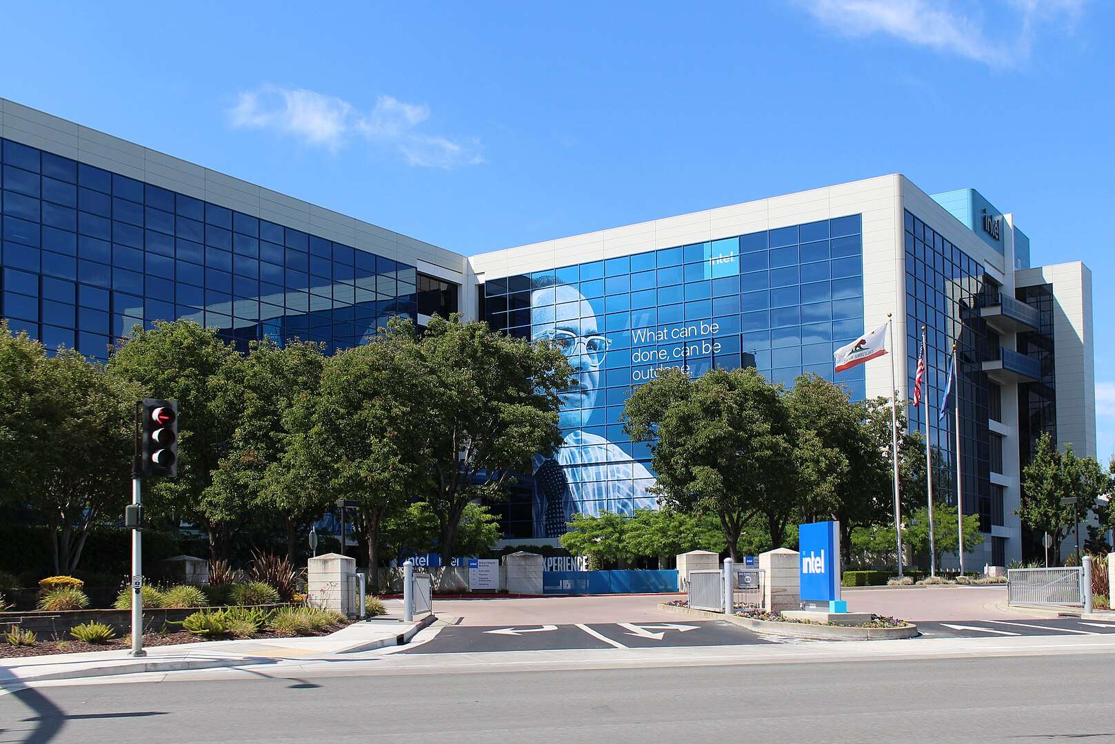
Intel has increased its new share offering from $15 billion to $20 billion after discovering higher-than-expected demand. The operation will allow the company to strengthen its balance sheet and finance capital investments at a time when it needs to expand advanced manufacturing and packaging capabilities to make Intel Foundry a more competitive alternative to TSMC. However, Intel has not officially allocated that $20 billion to specific new factories yet.
The key points of Intel’s capital increase in 20 seconds
- Intel has increased its share offering from $15 billion to $20 billion.
- It will issue 210.5 million shares at a price of $95 each.
- The funds may be used for capital investments and working capital, among other purposes.
- Intel is simultaneously expanding advanced manufacturing and packaging.
- The battle with TSMC includes processes like 18A and 14A, but also EMIB-T and Foveros.
The expansion involves issuing 210.5 million new shares at $95 each, which dilutes current shareholders’ stakes. Intel expects to net around $19.7 billion after expenses. The company initially announced a $15 billion offering but later decided to raise it to $20 billion.
Intel has explained that it will use the proceeds for general corporate purposes, including capital investments and working capital. Therefore, it would be incorrect to state that the entire $20 billion is solely for building or expanding factories.
The timing of these funds is highly relevant. Intel is increasing industrial investments in the U.S. and Europe, developing 18A and 14A processes, and expanding its packaging technologies to compete for major AI accelerators.
Intel 18A is already producing chips, and 14A will be the next test
The first piece of this strategy is Intel 18A, an advanced process where the company aims to regain technological competitiveness in manufacturing.
Intel confirmed in June that 18A will enter production in 2025. The process features two particularly important technologies: RibbonFET and PowerVia. RibbonFET replaces the previous FinFET transistors with a Gate-All-Around (GAA) architecture, while PowerVia delivers power to the backside of the chip.
The company is already working on its evolution.
Intel 18A-P has entered risk production, a phase before commercial high-volume manufacturing. Intel presents this variant as an evolution compatible with 18A design rules, aimed at improving performance without requiring customers to redesign from scratch.
Next will come Intel 14A.
This node will be especially important for Intel Foundry because the company needs to secure major external clients, not just manufacture its own processors. Intel has adopted a more disciplined investment policy under the leadership of Lip-Bu Tan and has conditioned future capacity expansion on demand that justifies it.
The challenge is no longer just demonstrating that Intel can develop advanced processes. It must convince companies that currently mainly produce with TSMC that it can deliver competitive technology, capacity, performance, costs, and volumes.
And TSMC isn’t standing still either.
Its N2 process started volume production in Q4 2025, and N2P is expected in H2 2026. TSMC claims N2P will offer approximately 5% more performance than N2 while maintaining their design rules.
Even more interesting for comparison with Intel is A16.
TSMC plans to have A16 ready for production in the second half of 2026. This process combines nanosheet transistors with Super Power Rail, its backside power delivery technology.
Compared to N2P, TSMC estimates A16 will deliver between 8% and 10% more performance at the same voltage, between 15% and 20% less power consumption at the same speed, and up to 1.10 times the chip density. These are manufacturer estimates and actual results will depend on each specific design.
The Taiwanese company particularly highlights high-performance computing (HPC) applications, precisely the market where AI accelerators and some of the largest, most profitable chips are concentrated.
EMIB-T and Foveros: manufacturing the transistor is no longer enough
The competition between Intel and TSMC has grown a second front each year: advanced packaging.
A modern AI accelerator might combine multiple compute chips, input/output interfaces, and high-bandwidth memory stacks (HBM).
Placing all these components in a single package and enabling communication at sufficient speed has become a technological challenge comparable in some aspects to chip manufacturing itself.
TSMC has built a significant position in this market through CoWoS (Chip-on-Wafer-on-Substrate) and SoIC (System on Integrated Chips). The enormous growth of AI accelerators has made advanced packaging capacity an important part of the supply chain.
Intel primarily responds with Foveros and the EMIB family.
EMIB, Embedded Multi-die Interconnect Bridge, uses small silicon bridges integrated into the substrate to connect chiplets only where needed. This avoids the need for a large silicon interposer covering the entire assembly.
EMIB-T advances this concept by incorporating Through-Silicon Vias (TSVs), vertical interconnects through silicon aimed at improving power distribution in large packages.
These dimensions begin to show how far the AI race has progressed.
Intel Foundry claims it can now build chip complexes roughly six times the size of a conventional reticle. In 2026, it aims to surpass eight reticles, about 6,800 mm², and by 2028, over twelve, around 10,000 mm².
Future designs could include 16 or more HBM4 or HBM5 stacks and at least 30 EMIB-T bridges, according to Intel’s roadmap.
TSMC is preparing even larger packages for 2028
TSMC is taking CoWoS down a similar path.
The company announced at its 2026 Technology Symposium that it is developing a CoWoS version equivalent to 14 reticles for 2028 production.
This size will enable integration of about 10 large compute chips and 20 HBM stacks within a single system. TSMC aims to surpass these 14 reticles by 2029.
Simultaneously, it continues developing SoIC for 3D stacking. TSMC plans to have SoIC A14 on A14 by 2029, with 1.8 times higher inter-chip connection density than N2 on N2.
This comparison helps explain why traditional fabs are only part of the necessary investment.
| Technology | Intel | TSMC |
|---|---|---|
| Current/next advanced process | 18A / 18A-P | N2 / N2P |
| Next generation | 14A | A16 / A14 |
| Backside power delivery | PowerVia / PowerDirect | Super Power Rail |
| 2.5D packaging | EMIB / EMIB-T | CoWoS |
| 3D stacking | Foveros | SoIC |
| Scale expected in 2028 | >12 reticles | 14 reticles |
The names do not directly correspond to equivalent technologies, and dates may shift as industrialization progresses, but they show both manufacturers are competing simultaneously in process technology and packaging.
Intel is also investing €5 billion in Ireland
The capital increase comes just weeks after Intel announced another substantial investment.
On July 13, the company confirmed an additional €5 billion for its Leixlip campus in Ireland, one of its main European manufacturing sites.
The funds will be used to modernize existing facilities, install new manufacturing tools, and increase capacity. Intel aims to produce Xeon 6 and the next-generation Xeon based on Intel 3 at this site.
This isn’t about building a new €5 billion factory from scratch. The investment leverages existing cleanrooms and modernizes current capacity, allowing Intel to boost production with a different expenditure than building a brand-new fab.
The company has already invested over €30 billion in Ireland since 1989 and employs around 4,900 people in Leixlip.
Meanwhile, the U.S. is concentrating significant efforts on advanced packaging. Intel has established New Mexico as one of its primary centers for technologies like Foveros and EMIB, essential for manufacturing the large packages required by upcoming generations of accelerators.
Intel needs to turn investments into customers and wafers
The $20 billion increase partly addresses Intel’s challenge: gaining greater financial flexibility to invest without excessively damaging its balance sheet through more debt.
In return, the operation results in dilution for current shareholders, as the number of shares outstanding increases.
The real test will come afterward.
Intel Foundry must fill its fabs with its own products and, most importantly, secure external manufacturing contracts that justify further investments. Building capacity without sufficient utilization would be particularly costly in an industry where advanced fabs can cost tens of billions of dollars.
Artificial intelligence presents a significant opportunity. Future accelerators will require more silicon, more HBM, and larger packages. But that same opportunity is prompting TSMC to aggressively expand its own capacity.
This is why the competition is no longer just about Intel 14A versus TSMC processes.
Any manufacturer aiming to secure a sizable share of future AI chips must offer competitive transistors, sufficient wafer supply, strong manufacturing performance, and the capacity to assemble chiplets and dozens of HBM stacks in ever-larger packages.
Intel has now strengthened its financial capacity to compete in this race. It remains to be seen whether it can turn this capital into actual industrial capacity used by real customers.
Frequently Asked Questions
How much money does Intel aim to raise with its capital increase?
Intel initially increased its planned operation from $15 billion to $20 billion, selling 210.5 million shares at $95 each.
Will Intel use the $20 billion to build factories?
There is no specific allocation for that purpose. Intel states the funds may be used for general corporate purposes, including capital investments and working capital. The operation coincides with significant investments in manufacturing and packaging, though.
What is Intel EMIB-T?
It is an advanced packaging technology that employs small silicon bridges to connect different chips within a package and incorporates TSVs to improve, among other things, power distribution. Intel aims to surpass packages equivalent to 12 reticles by 2028.
What is TSMC planning for advanced packaging?
TSMC is expanding CoWoS and expects to have solutions up to 14 reticles by 2028, capable of integrating about 10 large compute chips and 20 HBM stacks. It also continues developing SoIC for 3D stacking.
