
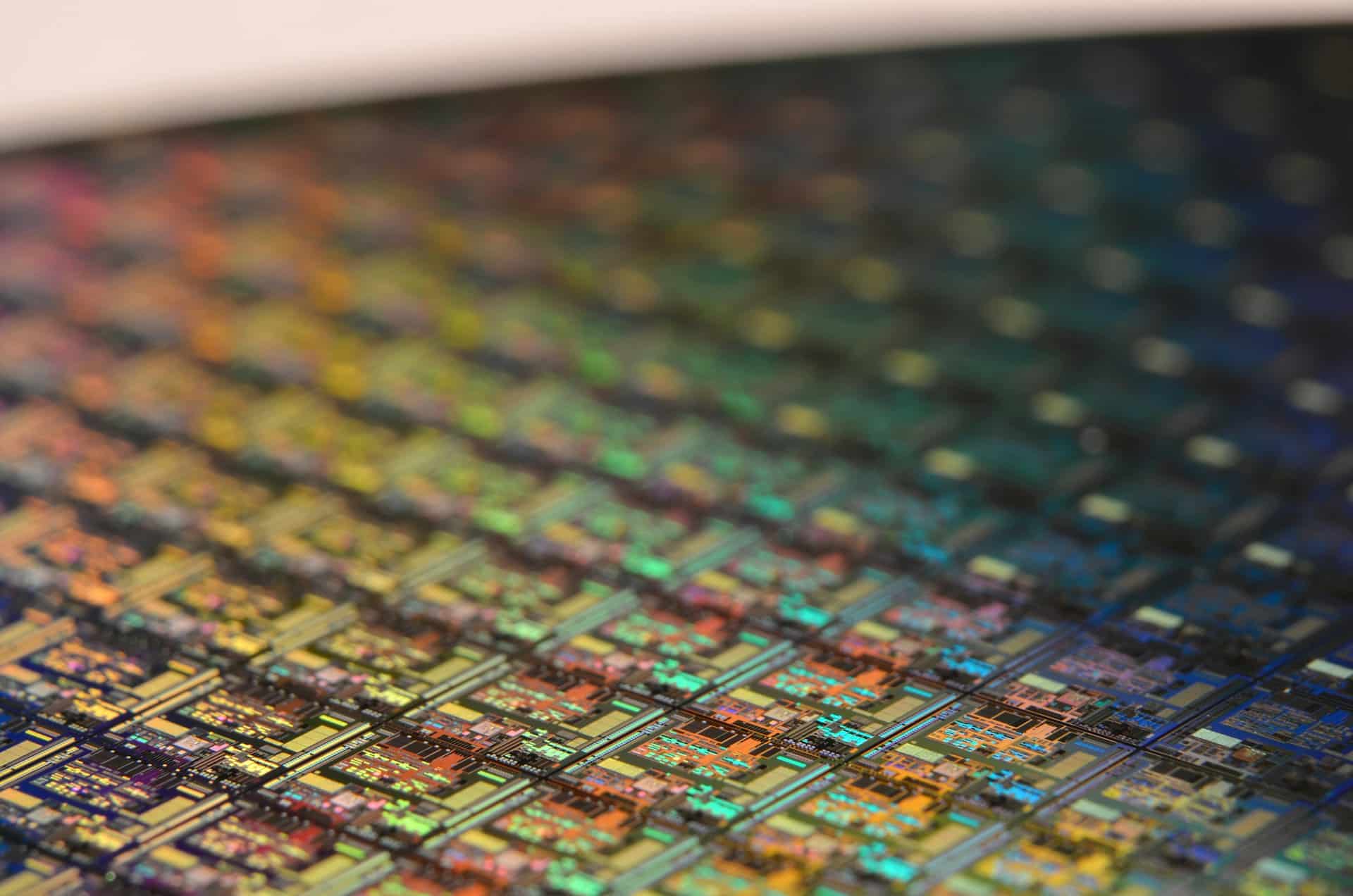
A developer linked to the Thru blockchain project says he used Meta’s Muse artificial intelligence (AI) agent to complete the physical design of a RISC-V-based system-on-chip (SoC) specialized in cryptographic operations. According to the data he shared, the work reached the generation of the GDSII file, which describes the circuit’s physical layout, at an estimated cost of about $2,000 in token usage. The design still needs to move toward actual manufacturing and prove its performance under real-world conditions.
The AI-designed RISC-V chip in 20 seconds
- The project uses Muse, a Meta AI agent, together with open hardware design tools.
- The SoC includes acceleration for algorithms such as SHA-256, SHA-512, Keccak, Ed25519, and secp256k1.
- Its author puts the design at around 61,590 logic cells, a target frequency of 100 MHz, and an estimated power draw of 20 milliwatts.
- The roughly $2,000 cost corresponds to AI usage, according to its author, not to full industrial development or chip manufacturing.
- The next step is getting access to shared manufacturing to produce the first silicon and check how it performs physically.
The experiment points to a possible reduction in the cost of some semiconductor design tasks, especially when AI agents are combined with automation tools that are already available. However, generating a physical design isn’t the same as having a manufactured, lab-validated processor ready to run a blockchain faster than any alternative.
What Muse Designed and How Far the Project Has Gotten
The announcement comes from a post by the user known as @bubbleboi, who shared an update on the project on October 13, 2026. In it, he says the design completed place-and-route with OpenROAD and produced a final GDS file. These steps lay out the logic cells across the circuit and define the metal connections linking its components.
GDSII is one of the formats used to describe an integrated circuit’s physical geometry. It’s an important step in preparing a chip for manufacturing, but its existence alone doesn’t show the design is ready for mass production. Before that, it has to pass the rules of the chosen manufacturing process, be prepared for submission to the fab, and have physical samples made to validate it.
According to the author, the design uses a RISC-V implementation as its base and includes blocks meant to accelerate common cryptographic operations. SHA-256 and SHA-512 are hash functions; Keccak is the cryptographic family behind SHA-3; Ed25519 is used for digital signatures; and secp256k1 is an elliptic curve used, among other things, in Bitcoin’s signature system.
The post puts the design at roughly 61,590 logic cells and cites a target operating frequency of 100 MHz, with a timing margin of about 4.5 nanoseconds. It also attributes 20 milliwatts of power consumption to the circuit and says it passed design rule checks (DRC) without detecting electrical issues at that stage.
These are results reported by the project’s lead and should be read with caution. Assessing real performance and power draw would require knowing the measurement conditions, the full circuit configuration, the manufacturing technology, and the results from an actual physical chip. A design-stage power estimate doesn’t guarantee the final silicon will hold to that figure.
The author also says the processor passed RISC-V compliance tests and floating-point validations, including ACT tests and 1.5 million Berkeley TestFloat vectors. The information shared doesn’t amount to independent certification of the whole SoC, nor does it show that all of its cryptographic functions are ready for production deployment.
The $2,000 Covers AI Usage, Not the Cost of Manufacturing the Chip
One of the most striking figures in the announcement is the roughly 100 million tokens consumed during the process, which the author translates into a cost of about $2,000. That figure illustrates the estimated cost of using the AI agent, but shouldn’t be confused with the total budget needed to develop and bring a processor to market.
Semiconductor design relies on a set of electronic design automation (EDA) tools, which are used to describe circuits, verify their behavior, and prepare their physical implementation. OpenROAD provides open-source tools for different stages of the digital design flow. Muse reportedly worked within that environment to complete tasks that traditionally require specialized expertise and a combination of technical tools.
AI can help generate hardware code, automate adjustments, and handle some of the repetitive work. But the outcome still depends on the starting architecture, the constraints applied, the tools available, and the ability to verify that the agent’s decisions are correct. In this case, the developer himself acknowledges he still wants to replace the third-party core used as a base and add vector instructions.
The full cost would also include engineering time, verification, manufacturing preparation, any needed corrections, and testing on the actual silicon. Access to specialized equipment and services would also have to be factored in. That’s why the $2,000 figure is an estimate attributed to AI usage, not a number that shows any company can develop a commercial chip for that amount.
The next goal is to find a multi-project manufacturing run, known as a Multi-Project Wafer (MPW). In this kind of service, several designs share the same silicon wafer, which helps split certain costs and lowers the barrier to entry for small projects. If the design passes the necessary checks and secures manufacturing space, the team will be able to move from a digital description to testing a physical circuit.
Thru Wants to Run Its Blockchain on a Specialized Processor
The project’s ultimate goal goes beyond showing that an AI agent can complete much of a chip’s physical design. Its lead wants to adapt the SoC to natively run the Thru blockchain, a layer-1 network that, according to the project’s own description, supports writing programs in languages such as C and Rust.
To do that, he plans to add vector instructions, remove the third-party core used as a starting point, and adapt the processor’s memory map to the network’s needs. The memory map determines how system resources are laid out and accessed, so its design can affect how software integrates with hardware.
The intent is to speed up operations that matter for running the blockchain. Even so, the goal of turning Thru into “the fastest blockchain in the world” is the developer’s own ambition, not a demonstrated result. Backing up that claim would require comparable tests against other networks, representative workloads, and measurements of performance, latency, power draw, and throughput.
The announcement also comes alongside new benchmarks designed to measure how capable AI agents are at chip design. An October 14 post credits Nvidia and ChipAgents with launching Build-A-Chip-Bench, a benchmark meant to assess how autonomously these systems can handle chip design tasks. According to that same post, the best-performing agent tested scored 16.6%.
That percentage needs to be read in light of the tasks involved, the evaluation criteria, and the specific version of the benchmark. It doesn’t mean agents can only complete 16.6% of any chip design, nor does it necessarily contradict the progress @bubbleboi announced: a specialized project, built on an existing core and with a narrow scope, isn’t the same as autonomously designing a full processor from scratch.
The experiment does raise a relevant question for the industry: how much engineering work can be automated when AI models operate on verifiable design tools. The answer will depend on whether these results can be reproduced, the quality of the manufactured hardware, and the costs that show up when moving from prototype to product.
Frequently Asked Questions
What chip did Meta’s Muse agent design?
According to the project’s author, Muse helped complete the physical design of a RISC-V-based SoC with accelerators for cryptographic algorithms such as SHA-256, Keccak, Ed25519, and secp256k1. The design still needs to move toward physical manufacturing.
How much did it cost to design the chip with artificial intelligence?
The developer estimates about $2,000 for roughly 100 million tokens consumed. That figure doesn’t necessarily include all the costs of engineering, manufacturing, validation, and commercial preparation.
Has the RISC-V processor already been manufactured?
The published information doesn’t indicate that a physical chip exists yet. The next announced step is seeking access to multi-project manufacturing to produce samples and check how the design actually performs.
Will the Thru blockchain become the fastest in the world thanks to this chip?
That’s the stated goal of the project’s lead, who wants to adapt the processor to run Thru natively. There are no comparative results yet showing the network will outperform all others in speed.
