The race for Artificial Intelligence is no longer decided solely by who manufactures the most GPUs or trains the largest models. By 2026, an increasingly evident bottleneck will be in memory: its bandwidth, capacity, and especially its availability. In this scenario, China is starting to reveal a strategy that directly challenges South Korea’s dominance in advanced memories: YMTC (Yangtze Memory Technologies) is working on a concept called High Bandwidth Flash (HBF), a proposal aimed at bringing NAND 3D closer to compute, filling a gap that HBM — crucial for AI accelerators — is beginning to expose.
The core idea is simple, though uncomfortable for the market: HBM (High Bandwidth Memory) offers excellent performance but is expensive, complex to package, and limited in total capacity near the GPU. As models grow, the challenge is no longer just “going fast,” but keeping大量 data close (weights, intermediate states, checkpoints, datasets, histories). That’s where YMTC argues that flash could play a new role: not as a distant SSD, but as stacked memory connected with a much higher bandwidth than conventional storage.
What is HBF and why is it coming into focus now?
HBF, as described by industry experts, aims to be a very high capacity flash memory integrated closer to the processor or accelerator, with an interconnection design intended to move data at speeds exceeding those of a typical SSD. Its promise is not to replace HBM in latency — which would be unrealistic — but to provide more capacity near computing and ease the pressure on the system’s most expensive memory pool.
The key point is that this is not an isolated idea or just a laboratory concept. Alongside Chinese initiatives, SanDisk and SK hynix announced a collaboration to standardize an HBF specification, describing it as a technology targeting AI workloads (particularly inference) with a very specific ambition: bandwidth comparable to HBM and 8 to 16 times more capacity, at a similar cost in their target market, with samples expected in 2026 and initial devices in 2027. In other words: the industry is literally trying to invent a new memory layer for the AI era.
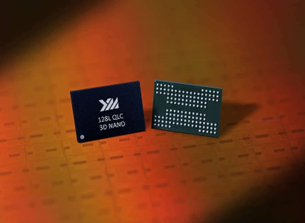
The Chinese plan: YMTC wants NAND to stop being “just SSD”
Against this backdrop, YMTC’s move is notable. According to Asian tech market sources, the company has disclosed advances in 3D NAND and its intention to develop HBF, leveraging the evolution of its Xtacking architecture. The Xtacking approach — in brief — involves separating the fabrication of the memory array and the logic/peripheral circuitry onto different wafers, then bonding them together. This strategy seeks to improve performance and scalability by optimizing each component separately.
The geopolitical reading is clear: YMTC operates under technological restrictions and strives to reduce dependency on foreign semiconductor technology. While South Korea dominates HBM and much of the “premium” memory powering AI GPUs, an “alternative memory” based on China’s NAND strengths could be a way out: more capacity near compute, albeit with trade-offs.
HBM vs HBF: the important comparison (and the nuance many overlook)
To understand why HBF is making waves, it helps to frame the issue practically:
- HBM (Stacked DRAM): Excellent for feeding GPUs with fast, low-latency data. It’s what enables real AI accelerator performance. But per-package capacity is limited, and its production depends on a complex supply chain (advanced DRAM, TSVs, 2.5D/3D packaging, interposers…).
- Flash (NAND): Cost-effective per GB and scalable in capacity. But its latency and storage nature make it unsuitable to replace DRAM at the “frontline” of compute.
HBF aims to position itself between these technologies: not intended to be GPU RAM, but a nearby layer that allows storing more data alongside the accelerator without always paying the “HBM tax.” In a world where each model iteration pushes for more checkpoints, versions, results, and histories—whether for reproducibility, auditing, or compliance—the pressure isn’t only computational: it’s also about near-memory storage and capacity.
The technical nuance separates a promising promise from a superficial headline: if HBF is used for data that requires DRAM-like latency, it will fail. If used as high-capacity memory for inference, staging, caching certain assets, or intermediate tiers, it could make operational and economic sense.
Why does this movement threaten Samsung and SK Hynix… even if HBF isn’t HBM?
Because controlling the de facto standard for AI memory isn’t just about selling HBM modules: it’s about defining who sets the memory standard. If the market accepts architectures where part of the “capacity problem” is solved with stacked flash, the debate shifts: how much HBM do certain scenarios really need per node? What portions of the budget can be shifted to other layers?
YMTC sees an opportunity here: China may not lead in cutting-edge HBM — yet — but it can lead a “new lane” in NAND, bonding, and advanced packaging. Moreover, if an ecosystem for HBF consolidates — and the fact that SanDisk and SK Hynix are already discussing standardization indicates efforts are underway — the supplier landscape reshapes itself.
What remains to be proven: reliability, software, and a critical question
Still, it’s important to temper expectations: HBF is a bold bet with serious challenges. Flash memory wears out, requires complex management, and its real performance depends heavily on controllers, firmware, and, crucially, how AI software adapts to a richer memory hierarchy. Success won’t be just “making a bigger cartridge,” but creating a system that makes moving data to this new tier worthwhile without sacrificing latency or energy efficiency.
The fundamental question is straightforward but decisive: Will HBF reduce the number of GPUs needed for a task, or just let us do more with the same? If it’s the latter, the market will adopt it anyway because, in AI, the clear incentive is to scale.
Frequently Asked Questions
What’s the difference between HBM and HBF in AI data centers?
HBM is stacked DRAM with very low latency and extremely high bandwidth to feed GPUs. HBF aims to add much more capacity using flash, with high bandwidth goals, but without replacing HBM for latency-sensitive tasks.
What is High Bandwidth Flash used for in inference of large models?
Primarily, it provides a “nearby” large-capacity layer to manage models, histories, and data that don’t need to always be in the fastest memory, improving cost-effectiveness and scalability in certain deployments.
Can HBF reduce dependence on HBM in the short term (2026–2027)?
It can relieve some pressure in scenarios limited by near-compute capacity but won’t eliminate the need for HBM for maximum performance. The actual impact will depend on available products and software adoption.
What are the risks of bringing flash memory close to an AI GPU or accelerator?
The main challenges are balancing latency, wear management, reliability, and the need for a software stack that efficiently exploits a more complex memory hierarchy without penalizing performance.
Sources: