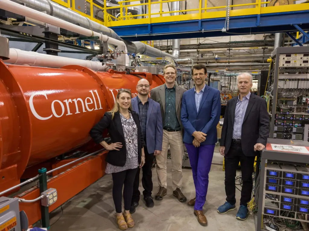
The battle for the next big leap in chip manufacturing has gained a new player. The startup based in the United States, xLight, backed by former Intel CEO Pat Gelsinger, has signed a Letter of Intent (LOI) with the U.S. Department of Commerce to receive up to $150 million in federal incentives under the CHIPS and Science Act. The goal: develop a new light source for extreme ultraviolet (EUV) lithography based on a free-electron laser (FEL), as an alternative to the current plasma laser sources used by ASML systems.
Although the LOI is not binding, it represents the first major move by CHIPS R&D office in the Trump era and places xLight at the center of the U.S. strategy to regain ground in a key technology currently dominated by Europe through ASML.
A symbolic agreement: money, action, and strategic influence
The announced deal includes up to $150 million in incentives to fund the construction, expansion, and demonstration of an FEL-based EUV source prototype at the Albany Nanotech Complex in New York, one of the flagship sites of the CHIPS program.
The Department of Commerce will not only provide funding: several official communications confirm that the government will also take an equity stake in the company, following the precedent set by other recent operations like the government’s stake in Intel.
For the U.S. administration, this move sends a clear message: control over a critical part of the advanced lithography supply chain, which has so far been in the hands of foreign suppliers. If xLight manages to integrate its technology with ASML’s EUV scanners or future competitors, the U.S. would gain direct influence over one of the industry’s most sensitive bottlenecks in semiconductor manufacturing.
What xLight aims to change: from plasma lasers to free-electron lasers
Today, ASML’s EUV machines generate 13.5-nanometer light using a complex plasma source: tin droplets are vaporized with a high-powered CO₂ laser, producing a plasma that emits EUV radiation. This system is highly sophisticated, expensive, difficult to maintain, and energy-intensive.
xLight proposes an alternative approach. Its plan involves building a EUV source based on a free-electron laser (FEL):
- A particle accelerator propels electrons to very high speeds using radiofrequency fields and magnets.
- These electrons are sent through a series of undulators (periodic magnetic structures) that force the electrons to oscillate and emit coherent high-intensity light.
- The system is tuned to generate EUV radiation at 13.5 nanometers, with the potential to scale to even shorter wavelengths within the soft X-ray range.
The key architectural feature of xLight’s design is the arrangement: the FEL would be located in a separate facility adjacent to the factory, not inside the cleanroom. From there, the EUV light would be guided through a mirror network with grazing incidence and rotation stations until reaching several wafer scanners; the company claims to be able to feed up to 20 EUV machines from a single FEL source.
More brightness, less power consumption, and ultrashort pulses
By eliminating the plasma conversion stage, xLight argues that its system can offer several advantages over existing sources:
- Higher brightness: more useful EUV photons per unit time, translating into more wafers processed per hour.
- Narrower spectrum, which would help improve the precision of patterning on silicon.
- Femtosecond pulses, relevant for fine-tuning line edges and reducing phenomena like stochastic roughness in the most advanced nodes.
- Improved energy efficiency, with internal estimates claiming up to an order of magnitude better performance than current EUV sources—something critical amid soaring electricity costs in large data centers and cutting-edge fabs.
Pat Gelsinger, now CEO of xLight, has directly linked this project to the “next era of Moore’s Law”: if a much more efficient EUV laser is achieved, factories could boost productivity, cut chip costs, and support the scaling toward smaller transistors for several additional nodes.
A high-risk experiment involving machines costing hundreds of millions
Despite enthusiasm from the Department of Commerce and the company itself, xLight’s technology is still in early stages. The company must demonstrate two tough things:
- That its FEL system operates stably and reproducibly under the demanding conditions of semiconductor manufacturing.
- That it can integrate with commercial EUV scanners of low and high NA (numerical aperture), machines that can cost between roughly $200 million and nearly $400 million each.
Convincing a major foundry to lend one or more of these high-end EUV scanners for experimentation will be challenging. The company plans to leverage the ecosystem at the Albany Nanotech Complex, home to one of the most advanced R&D centers in the CHIPS program, specifically equipped for EUV development.
There’s also a sensitive geopolitical aspect. xLight collaborates with multiple national laboratories under the Department of Energy (DOE), and parts of its technology may be classified. This would help the U.S. safeguard certain capabilities from foreign adversaries, but could also slow global adoption by complicating export or full integration outside the U.S.
Another move in the race for lithography control
The announcement arrives at a time when Washington aims not only to attract chip factories but also to recover critical parts of the supply chain, from materials to manufacturing equipment. EUV lithography is arguably the most strategic link: without these machines, cutting-edge chips cannot be produced.
With xLight, the Trump administration sends a dual message. On one hand, it leverages the financial and regulatory infrastructure of the CHIPS Act, previously used to support “disruptive” technology development. On the other, it asserts influence through direct stakes in key companies, from Intel to startups like xLight, in an effort to ensure the next generation of manufacturing tools is born under U.S. leadership.
If successful, this project could diminish ASML’s current dominance by increasing U.S. dependence on the most complex part of their systems: the light source. If it fails, it will be another reminder of how challenging it is to push the physical and economic limits of advanced lithography. For now, the experiment has received a $150 million boost and industry attention.
Image and source: xlight.com


