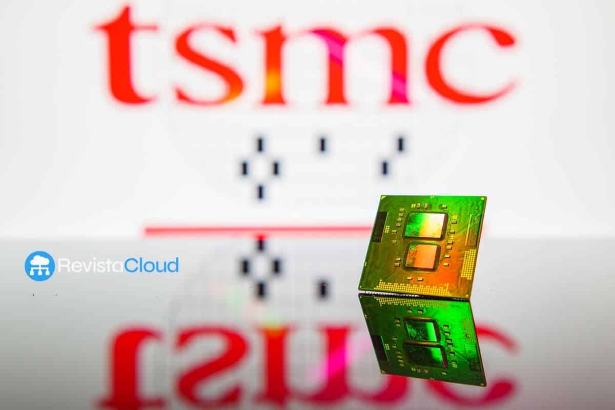
From the heart of Silicon Valley, TSMC has unveiled details of its next major technological bet: the A14 node, a direct evolution of the N2 process aimed at enhancing high-performance computing, generative artificial intelligence, and future mobile devices. The announcement was made during the North America Technology Symposium 2025, the Taiwanese company’s most significant event on its international calendar.
With this presentation, TSMC confirms its roadmap in semiconductor technology, where the A14 node promises a 15% improvement in speed at the same energy consumption, or a 30% reduction in energy consumption while maintaining the same speed, along with a 20% increase in logical density compared to its predecessor.
A14, a next-generation node with High-NA EUV
Designed to enter production in 2028, the A14 will utilize high numerical aperture (High-NA) EUV scanners for the first time and evolve the nanosheet transistor architecture that debuted with the N2. Additionally, it will implement an advanced version of the NanoFlex™ standard cells—renamed NanoFlex™ Pro—which provide greater energy efficiency and design flexibility for AI and compute-intensive chips.
Key improvements of the A14:
- +10-15% speed compared to N2 (at the same consumption)
- -25-30% consumption compared to N2 (at the same speed)
- +23% logical density
- Mass production without BSDPN: H2 2028
- Version with BSDPN (Super Power Rail): available in 2029
CoWoS, SoW-X, and a complete ecosystem for AI and HPC
TSMC did not limit itself to the A14 node. At the symposium, it also revealed significant advancements in advanced packaging and systems on wafer, such as:
- CoWoS with 9.5 reticles: in production by 2027, supporting up to 12 HBM stacks and advanced logic.
- SoW-X (System-on-Wafer Extended): an evolution of its innovative TSMC-SoW™, capable of delivering 40 times more computing power than conventional CoWoS.
- COUPE™: an integrated photonic engine for optical computing.
- Integration of IVR (integrated voltage regulator) with 5 times higher vertical power density for AI.
These technologies are designed to support everything from the most demanding generative AI systems to cloud infrastructures and military and automotive applications.
RF, automotive, and IoT: a portfolio beyond the node
Meanwhile, TSMC also introduced specific improvements for key sectors:
- N4C RF: its new radio frequency technology for smartphones and edge devices with AI, which reduces consumption and area by 30% compared to N6RF+.
- N3A (Automotive Grade): in the final qualification phase AEC-Q100 for ADAS and autonomous vehicle applications.
- N6e and N4e: ultra-low consumption processes aimed at IoT for smart devices with local AI and limited battery.
EUV High-NA and the competitive landscape with Intel
The arrival of the A14 node comes in an increasingly competitive environment. Intel is already working on its Intel 14A node, expected for 2026-2027, which will also use High-NA EUV and a new generation of PowerVia (BSDPN). Unlike Intel, TSMC has chosen to launch its node first without BSDPN and then evolve to the version with Super Power Rail, which could delay its initial mass adoption.
In any case, the technological leap from N2 to A14 will be crucial, not so much for linear advances in PPA (Performance, Power, Area), but for the possibility of combining these nodes with chiplet architectures, optical interconnects, and AI-specific silicon.
Conclusion
With the A14, TSMC not only responds to industry demands in terms of power and efficiency but also consolidates its long-term technological leadership. Although advancements in PPA scalability are beginning to show signs of fatigue, the key to the future seems to lie in vertical integration, the co-optimization of design and technology, and in providing a complete ecosystem of computing, communication, and storage.
We will have to wait until 2028-2029 to see these chips in volume, but the message is clear: the battle for supremacy in AI and HPC is no longer fought only in nanometers but in the complete architecture of the system.
More Information at Semiwiki