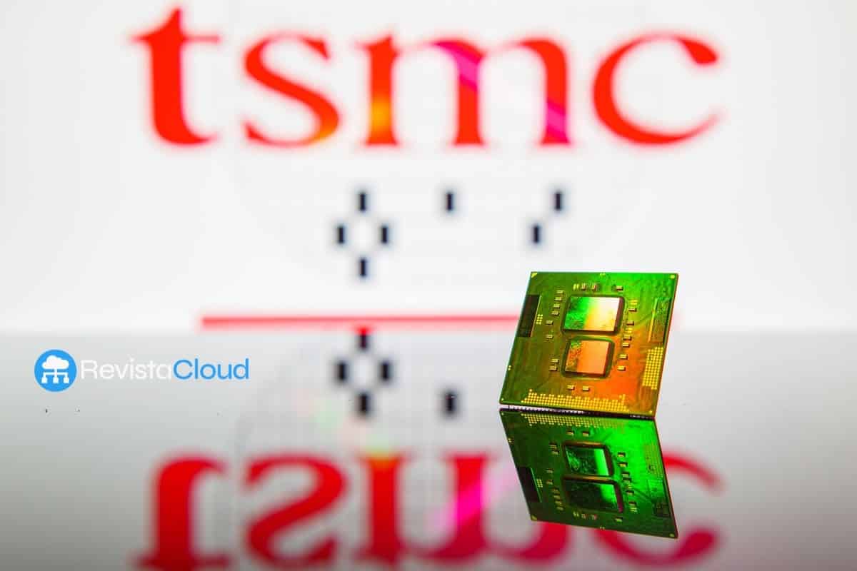
TSMC has once again made it clear that the AI race isn’t just about designing GPUs, ASICs, or accelerators. It’s also decided in factories, in advanced packaging, and in the capacity to integrate increasingly more HBM memory alongside large compute blocks. At its Taiwan Technology Symposium 2026, the company raised its forecasts: demand for wafers for AI accelerators could grow 11 times between 2022 and 2026, while the global semiconductor market might surpass $1.5 trillion by 2030.
This figure is significant because TSMC no longer discusses AI as a one-time investment cycle but as the main growth driver for the industry in the coming years. The company, which manufactures chips for many of the industry’s major players, is adapting its roadmap to a market where models are larger, memory consumption is skyrocketing, and advanced packaging has become as critical as the manufacturing node itself.
From 2 nm to Packaging: AI Demands More Than Transistors
For years, the semiconductor conversation focused almost entirely on node advancements: 7 nm, 5 nm, 3 nm, 2 nm. That race remains important, but it’s no longer enough. In AI accelerators, performance depends on a broader combination: more densely packed transistors, high-bandwidth memory, fast interconnects, energy efficiency, and the ability to package multiple chips within a single system.
TSMC forecasts that capacity for its most advanced processes, including 2 nm and A16, will grow at a compound annual rate of 70% between 2026 and 2028. The company also expects its CoWoS capacity—the advanced packaging technology used in many AI accelerators—to grow over 80% annually between 2022 and 2027.
| Area | Forecast or Key Data |
|---|---|
| Demand for wafers for AI accelerators | 11 times more between 2022 and 2026 |
| Global semiconductor market | Over $1.5 trillion by 2030 |
| 2 nm and A16 capacity | 70% CAGR between 2026 and 2028 |
| CoWoS capacity | Over 80% CAGR between 2022 and 2027 |
| New fab and packaging phases in 2026 | 9 phases planned |
| CoWoS planned for 2028 | 14 reticles and up to 20 HBM stacks |
| CoWoS planned for 2029 | Over 14 reticles and up to 24 HBM stacks |
| SoW-X planned for 2029 | Up to 64 HBM stacks |
The underlying message is clear: AI is forcing TSMC to grow in multiple directions simultaneously. On one hand, it needs more capacity at advanced nodes. On the other, it must expand CoWoS, SoIC, silicon photonics, and wafer-scale integration technologies. Major clients aren’t just asking for more chips; they demand complete systems capable of moving data at ever-faster speeds.
CoWoS, SoIC, and COUPE: The Data Movement Bottleneck
The key technical protagonist is CoWoS, a technology that enables placement of large computing dies and HBM memory on an interposer to reduce electrical distances and increase bandwidth. TSMC already produces 5.5-reticle versions, which, according to published data, achieve 98% manufacturing yields. The next stage will be much more aggressive: a 14-reticle version in 2028, capable of integrating around 10 large compute dies and 20 HBM stacks, followed in 2029 by a version over 14 reticles with up to 24 stacks.
This evolution matters because HBM has become one of the most valuable hardware pieces for AI. Accelerators not only need to perform more operations; they need to constantly feed their cores with data. If memory lags, the chip’s theoretical performance sits underutilized. That’s why companies like NVIDIA, AMD, Broadcom, Google, Microsoft, Amazon, and other accelerator designers are increasingly dependent on the availability of HBM and TSMC’s packaging capacity.
TSMC is also advancing its SoIC technology—its 3D integration solution. According to information from the symposium, SoIC offers 56 times higher interconnection density and five times better energy efficiency compared to CoWoS from 2015. The roadmap includes bonding pitches of 6 microns, evolving toward 4.5 microns in the A14 generation, enabling stacking of components with denser connections and lower power consumption.
Another important piece is COUPE, TSMC’s photonics technology. The company reports that its first 200 Gbps Micro Ring modulator based on COUPE entered production this year. The promise is to reduce latency and power consumption compared to traditional copper interconnects—an increasingly critical factor in AI systems where moving data between chips, memory, and servers consumes a growing share of energy.
Arizona and the Geopolitical Dimension of Expansion
TSMC’s growth plan isn’t limited to Taiwan. Its operations in Arizona continue to gain momentum. The first factory is already in production; the second will begin equipment installation in the second half of 2026; the third is under construction, and the company plans to start work this year on a fourth factory and its first advanced packaging facility at that site.
TSMC expects Arizona’s output to increase 1.8 times year-over-year in 2026, with yields comparable to Taiwan. This figure has both an industrial and a political interpretation. The U.S. aims to reduce reliance on Asia for advanced semiconductors, while major North American clients seek a closer supply chain for AI chips, defense, cloud, and high-performance computing.
However, the core of TSMC remains Taiwan. The Asia-Pacific region continues to house a significant portion of advanced capacity consumption and ecosystem development. According to data shared at the symposium, regional customers used over 2.1 million 12-inch wafer equivalents last year—a figure TSMC compared to a tower taller than Taipei 101.
AI Pushes TSMC Toward Complete Systems
The most ambitious part of the roadmap appears with System on Wafer (SoW). TSMC has already brought logical SoW into production in 2024 and aims for SoW-X with integrated HBM by 2029. This technology could incorporate up to 64 HBM stacks and 16 CoWoS modules on wafer sizes exceeding 40 reticles. It’s a scale that surpasses the traditional “chip” concept and approaches a full system built on a wafer.
This kind of integration makes sense for AI because future models will require more memory, lower latency, and greater efficiency per watt. The trend is toward larger packages, closer to the physical manufacturing limits, with increasingly sophisticated interconnections. The industry’s scaling isn’t just about smaller nanometers anymore; it’s about connecting more intelligence in less space and with less energy—by stacking memory, connecting chips, and replacing copper links with optical ones where needed.
The opportunity for TSMC is enormous, but so are the risks. CoWoS remains one of the most scrutinized bottlenecks for AI clients. If demand continues to grow as forecasted, any delay in packaging capacity could impact the availability of accelerators, servers, and entire clusters. Additionally, reliance on a few HBM suppliers, lithography tools, and advanced materials makes the entire supply chain more vulnerable to geopolitical tensions or supply disruptions.
The symposium’s clear conclusion is that TSMC doesn’t just want to be the foundry manufacturing the most advanced transistors. It aims to be the physical platform on which the AI infrastructure of the next decade is built. This includes 2 nm and A16 nodes, but also CoWoS, SoIC, photonics, advanced packaging, and wafer-scale systems.
If forecasts hold, the AI chip of 2029 won’t look much like today’s accelerators. It will be larger, with much more memory, more dependent on packaging than a single piece of silicon, and will force data centers to think of the entire system as an extension of the package itself. The race isn’t just about making smaller transistors anymore; it’s about connecting more intelligence in less space and with lower energy consumption.
Frequently Asked Questions
What has TSMC announced regarding AI demand?
TSMC predicts that wafer demand for AI accelerators will grow 11 times from 2022 to 2026, driven by data center expansion and ever-larger models.
What is CoWoS?
CoWoS is TSMC’s advanced packaging technology that integrates compute dies and HBM memory in a single package via an interposer, increasing bandwidth and reducing interconnection distances.
Why are the 24 HBM stacks planned for 2029 important?
Because they will enable feeding AI accelerators with significantly more memory and bandwidth within the same package—crucial for larger models and high-performance computing workloads.
What role does Arizona play in TSMC’s strategy?
Arizona is part of TSMC’s international expansion. The first factory is operational, the second will install equipment in 2026, and the company plans to continue expanding fabs and advanced packaging facilities in the region.
via: trendforce