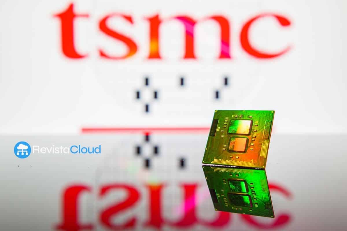
Memory shortage is once again shifting the pieces in Taiwan. According to information published by Taiwanese financial media, TSMC may have included Winbond in its supply chain for future AI chips based on 3D Wafer-on-Wafer (WoW) integration—a technology that stacks memory wafers on logic wafers through hybrid bonding. The operation has not been publicly confirmed by the companies, but it aligns with a very clear trend: AI is turning memory and advanced packaging into the new focal points of the semiconductor industry.
The most immediate takeaway is about supply. TSMC has historically worked with major global memory manufacturers like Samsung, SK Hynix, and Micron, but pressure on DRAM, HBM, and server memory has pushed the entire industry to seek more diverse and closer sources. In this context, Winbond could supply DRAM wafers for TSMC to integrate with its logic wafers in advanced architectures.
The deeper implication is industrial. Taiwan doesn’t want to be just the place where the most advanced logic chips are manufactured. It also aims to strengthen a local ecosystem of memory, packaging, assembly, testing, servers, and AI systems. If confirmed, Winbond’s involvement in these projects would represent a significant leap for a company better known for specialty memories, niche DRAM, and NOR Flash than for being at the core of AI accelerators.
What is WoW and why does it matter in AI chips
Wafer-on-Wafer (WoW) is a 3D integration technique where two full wafers are aligned and bonded vertically. Instead of connecting chips via long traces, interposers, or boards, logic and memory can be stacked with thousands or millions of microscopic connections. The key is to reduce the distance data must travel.
In artificial intelligence, this distance really matters. Large models require not just computation but also massive data movement between memory and processors. As accelerators become more powerful, the bottleneck shifts to bandwidth, latency, and the energy needed to move data—known as the “memory wall.”
Technologies like HBM, CoWoS, SoIC, and WoW seek to address this limit from different angles. HBM places high bandwidth memory close to the processor. CoWoS enables large chips and memory to be integrated on an interposer. SoIC and hybrid bonding go further, with extremely dense connections between chips or wafers. WoW fits within this family of solutions aiming to shorten the path between logic and memory.
| Technology | What it does | Role in AI |
|---|---|---|
| HBM | Stacks high bandwidth DRAM | Provides GPUs and accelerators with close, high-memory capacity |
| CoWoS | Integrates logic and memory on an interposer | Current foundation for many advanced AI accelerators |
| SoIC | High-density 3D chip-to-chip bonding | Reduces distance, power consumption, and improves bandwidth |
| WoW | Stacks logic wafer and memory wafer | Seeks more direct, dense integration for future architectures |
| Hybrid bonding | Bonds surfaces with very fine copper connections | Enables more interconnections with less power than traditional methods |
The main difference with WoW is that it works at wafer scale. This can offer advantages in density and alignment when pieces fit well, but it also presents significant manufacturing performance challenges. If a memory wafer or logic wafer has defects, the impact can be greater than in more flexible chiplet schemes. That’s why selecting the right memory partner is crucial: stable processes, quality control, and integration capability are essential.
Winbond: From niche memory to a potential AI player
Winbond does not compete at the same level as Samsung, SK Hynix, or Micron in HBM. Its profile has traditionally been different. The Taiwanese company specializes in products like Specialty DRAM, Mobile DRAM, Code Storage Flash, and NOR memories, with presence in communications, automotive, industrial, consumer, and peripheral markets. This positioning has made it less visible than Korean and American giants, but it has also given it experience in specific memories and mature processes.
For this reason, the potential collaboration with TSMC is particularly interesting. It wouldn’t imply that Winbond will replace major HBM suppliers for current AI accelerators; rather, it could serve as a complementary route where TSMC needs memory wafers suitable for 3D integration and aims to build more resilience within Taiwan.
From TSMC’s perspective, this move makes strategic sense. The company is the primary logic wafer manufacturer for Nvidia, AMD, Apple, Broadcom, Qualcomm, and much of the AI ecosystem. But the final performance of an accelerator no longer depends solely on the node process. It also depends on memory, advanced packaging, substrates, interconnection, power, and assembly capabilities. A bottleneck in any of these layers can prevent delivery to the customer.
| Stakeholder | Current strengths | Gains from WoW collaboration |
| TSMC | Advanced logic, SoIC, CoWoS, 3D integration | Greater control over close memory supply and local sourcing |
| Winbond | Specialty DRAM, Mobile DRAM, NOR Flash, Taiwanese manufacturing | Entry into AI, HPC, and server applications |
| Major AI clients | Need for more bandwidth and lower power | New options for logic-memory integration |
| Local Taiwanese ecosystem | Foundries, OSAT, servers, boards, and assembly | Greater autonomy and reduced external dependency |
For Winbond, this would be a strategic leap. Participating in an AI supply chain with TSMC could open doors in servers, HPC, and platforms where memory stops being a commodity component and starts to become part of the system design. While it won’t instantly make Winbond the leader in AI memory, it could position it much closer to the architecture’s core.
AI drives Taiwan to reinforce the entire supply chain
The broader context is the global memory shortage. The demand for HBM for GPUs and accelerators has led Samsung, SK Hynix, and Micron to prioritize high-value capacity. This has strained other categories of DRAM and driven prices in older segments. Scarcity is even affecting mature generations because manufacturers are reallocating wafers toward more profitable products.
TSMC is also under pressure. Its advanced nodes and CoWoS packaging have become scarce resources for AI. The company is accelerating investments, but demand growth is ahead. Relying solely on external memory suppliers or highly concentrated supply chains increases operational risk.
Taiwan has a clear advantage: it concentrates many critical parts of the semiconductor ecosystem. TSMC for logic manufacturing, ASE and others for assembly and testing, Quanta, Foxconn, Wistron, and Inventec in servers, along with several local memory manufacturers potentially entering advanced integration. The natural strategy is to further close the gaps within the island.
This doesn’t eliminate external dependence. EUV lithography equipment from ASML, critical materials from Japan, HBM memory dominated by Korea and the US, and much of the end demand from US hyperscalers—all remain outside Taiwan’s borders. But each layer Taiwan can strengthen locally reduces vulnerability and boosts bargaining power.
Winbond’s potential entry into WoW should be viewed not as a complete replacement for major memory vendors, but as an attempt to build redundancy, flexibility, and local expertise in a technology that could be crucial for the next generation of AI chips.
From current CoWoS to more aggressive 3D packaging
Today, CoWoS packaging is a foundation of the most advanced AI accelerators. It allows logic chips and HBM stacks to be placed on a silicon interposer, offering high bandwidth and density. But the industry is already looking toward even denser solutions with more vertical integration and shorter electrical paths.
TSMC has been developing SoIC for years as part of its 3DFabric platform. The company highlights that these technologies enable die-to-die connections with high density, smaller form factors, more bandwidth, improved signal integrity, and lower power consumption compared to conventional packaging methods. WoW is part of this trend alongside other schemes like Chip-on-Wafer.
The direction is clear: AI chips will increasingly evolve from single large dies connected to external memory into three-dimensional systems with logic, memory, interconnects, power, and cooling integrated into a unified architecture. In this transition, the boundary between foundry, memory, and packaging becomes more blurred.
If TSMC and Winbond progress with WoW, the goal isn’t just more DRAM. It’s about positioning memory where it has the most value—right next to the logic—reducing latency and improving energy efficiency. This is one of the major battlegrounds in AI.
The broader warning for the industry is that while many see GPU shortages as a Nvidia issue, the real bottleneck is more widespread. Memory, packaging, wafers, equipment, power, substrates, and integration capacity all play a role. AI scaling isn’t only about designing better chips; it’s about building a supply chain capable of manufacturing them.
Taiwan appears to recognize that the next advantage won’t be just producing a component but coordinating many. In that coordination, local memory could shift from a secondary role to a strategic component.
FAQs
What have TSMC and Winbond agreed upon?
According to Taiwanese economic press, both companies would collaborate on 3D Wafer-on-Wafer integration, with Winbond providing DRAM wafers and TSMC stacking them with logic wafers for AI applications. No official public confirmation has been issued by either company.
What is Wafer-on-Wafer?
It’s a 3D integration technique that bonds two complete wafers—such as one logic and one memory—using very dense connections to reduce distance, latency, and power consumption.
Why does this matter for AI?
Because AI accelerators need to transfer enormous amounts of data between memory and processor. Bringing memory closer to logic helps to mitigate the “memory wall.”
Will Winbond compete with SK Hynix, Samsung, or Micron in HBM?
Not necessarily. Its role would likely be complementary—focused on memory wafers for advanced integration—not directly replacing the leading HBM suppliers.
What does Taiwan stand to gain from this collaboration?
It strengthens a local memory and 3D integration supply chain for AI, reduces dependence on external sources, and enhances the resilience of its semiconductor ecosystem.
via: money.udn