The leap to 2 nanometers has become synonymous with budgetary vertigo for the entire industry. In recent months, wafers priced around $30,000 each, manufactured by TSMC, have been discussed—figures hard to swallow even for giants like Apple, Qualcomm, or MediaTek. However, new rumors from industry sources in China suggest a slightly less dramatic scenario: the 2 nm N2 node would offer limited improvements in power, performance, and area (PPA), but would also entail a more contained increase in costs compared to the current 3 nm generation.
According to the well-known leakster “Smart Chip Insider” on Weibo, several chipsets based on TSMC’s 2 nm process are progressing “as normal” toward their market debut in 2026. The key point is that these PPA improvements would be much more moderate than in previous generations, which would reduce the cost leap per wafer compared to the 3 nm N3P node that currently defines the high end.
Less PPA jump, less price jump
In the semiconductor world, each new generation is evaluated in terms of PPA: Performance, Power, and Area. The rumor places N2 at approximately a 15% performance improvement over N3E and up to a 30% reduction in power consumption, significant figures but far from the large jumps seen in historical node transitions.
Additionally, there’s N2P on the table, a slightly more advanced variant of N2, with barely an extra 5% performance gain. The industry’s takeaway is clear: the practical difference between a well-optimized 3 nm N3P chip and a 2 nm N2 chip will not be as vast as in previous transitions.
This moderation in PPA has a direct consequence: the additional cost per wafer compared to 3 nm would be less than initially feared. The $30,000 figure has likely been inflated by speculation, and while 2 nm will still be expensive, the leap will not be as explosive. For SoC manufacturers, accustomed to a mix of more costly wafers and increasingly expensive memories, any relief is welcome.
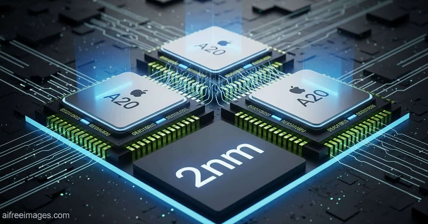
Apple to lead with the A20, followed by Qualcomm and MediaTek
Currently, all eyes are on Apple as the launch customer for N2. The upcoming Apple A20 and A20 Pro, likely destined for high-end iPhones in 2026, are expected to be built on this 2 nm node. The company has been unveiling new process generations with its mobile SoCs for years, and this move aligns with its strategy to maximize efficiency and battery life in mobile and portable devices.
Following suit, major Android ecosystem players are associated with migrating to N2P, the slightly more advanced variant of the 2 nm node, for chips like the Snapdragon 8 Elite Gen 6 and Gen 6 Pro, or the Dimensity 9600. These flagship chips would also incorporate LPDDR6 memory, significantly more expensive than the current LPDDR5X.
The parallel increase in memory costs is an important aspect of the problem: even if TSMC manages to contain wafer costs, manufacturers will need to deal with significantly more expensive DRAM modules, driven by AI demand and data centers. Therefore, balancing technological advancement against total system cost (silicon + memory + packaging) is becoming increasingly delicate.
3 nm versus 2 nm: squeezing silicon ever more difficult
An underlying message from this rumor is that the era of significant performance jumps per node may be reaching its limit. As the industry approaches physical limits and adopts architectures like nanosheets and GAAFETs, each additional improvement requires colossal investments in R&D and equipment, while incremental benefits diminish.
In this context, a 15% performance boost and a 30% power reduction compared to N3E might be enough to justify moving to 2 nm in very high-end products, but perhaps not for volume lines where price is king. Many manufacturers might opt to maximize N3P in intermediate segments, reserving N2 and N2P for flagship, advanced AI, or high-margin specialty applications.
There is also a growing trend to combine node improvements with other strategies: more efficient CPU/GPU architectures, dedicated AI accelerators, advanced packaging (chiplets, 3D stacking), energy-saving algorithms, and software optimization. The node is no longer the sole protagonist in the equation.
What does this mean for mobile and device prices?
The big question from end users remains: will I pay much more for my next mobile or laptop? If this scenario is confirmed, the outlook might be a bit less pessimistic than initially feared.
- If the cost per wafer for N2 increases but not exorbitantly, manufacturers may have more room to absorb part of the increase through design optimization and production scaling.
- The real bottleneck might be LPDDR6 memory and other key components (storage, RF modules), which are highly sensitive to demand from AI and data centers.
- We’re likely to see the first 2 nm SoCs in “ultra-premium” devices with very high prices, while the flagship “normal” range continues relying on 3 nm N3P for longer.
In other words: 2 nm will be a marketing and efficiency argument, but not necessarily lead to a sudden price spike across the entire product range… at least not immediately.
A more progressive than revolutionary 2 nm
This rumor makes clear that TSMC’s N2 node might be more evolutionary than revolutionary. The market will continue to see 2 nm as cutting-edge, but the actual leap compared to 3 nm will be more nuanced than the jump from 7 nm to 5 nm, for example.
For Apple, Qualcomm, MediaTek, and other clients, the message is twofold:
- On one hand, they will gain efficiency and performance improvements that enable longer battery life, more AI power, and higher transistor density.
- On the other, the additional wafer cost might be contained enough not to completely blow up the pricing structure of their most advanced products.
In a context where AI is stressing the entire supply chain—from GPUs to DRAM—the fact that the move to 2 nm isn’t as traumatic as feared is, in itself, good news for the ecosystem.
Frequently Asked Questions (FAQ)
How much will a TSMC 2 nm wafer really cost, and how does it affect chip prices?
The rumored figure is around $30,000 per wafer, but recent leaks suggest these estimates might be inflated, and the actual increase over 3 nm will be more moderate. Still, wafer costs will remain high, and SoC manufacturers will likely reserve this node for higher-margin or ultra-premium products, at least in the initial wave of adoption.
What performance and power differences are expected between 3 nm (N3E/N3P) and 2 nm (N2/N2P)?
Leaks indicate about a 15% performance improvement and up to 30% power reduction for N2 over N3E. N2P would add roughly 5% more performance. These are meaningful gains, but far from the significant jumps of previous generations, reinforcing the idea that 2 nm will be more of an incremental evolution than a full breakthrough compared to 3 nm.
Which manufacturers will be first to adopt TSMC’s 2 nm node?
All signs point to Apple as the launch customer with its upcoming A20 and A20 Pro chips expected in 2026. Subsequently, Qualcomm and MediaTek are likely to migrate to N2P with chips like Snapdragon 8 Elite Gen 6/Gen 6 Pro and Dimensity 9600, targeting high-end Android devices. Later, other clients might incorporate 2 nm in AI chips, data centers, or other high-margin applications.
Why could LPDDR6 memory be a concern even if 2 nm wafers don’t see a price spike?
Even if TSMC manages to keep wafer costs in check, LPDDR6 memory—the type that will accompany these SoCs—will be significantly more expensive than current LPDDR5X. The soaring demand for DRAM and NAND driven by AI infrastructure and data centers is driving up memory prices globally. This means the overall platform cost (SoC + memory + packaging) will continue to rise, and manufacturers will need to carefully decide which segments and products make sense to pair 2 nm with LPDDR6.
Sources:
Rumors and data shared by “Smart Chip Insider” and “Digital Chat Station” on Weibo, as well as industry information on TSMC’s roadmap and plans for Apple, Qualcomm, and MediaTek adoption.
via: wccftech