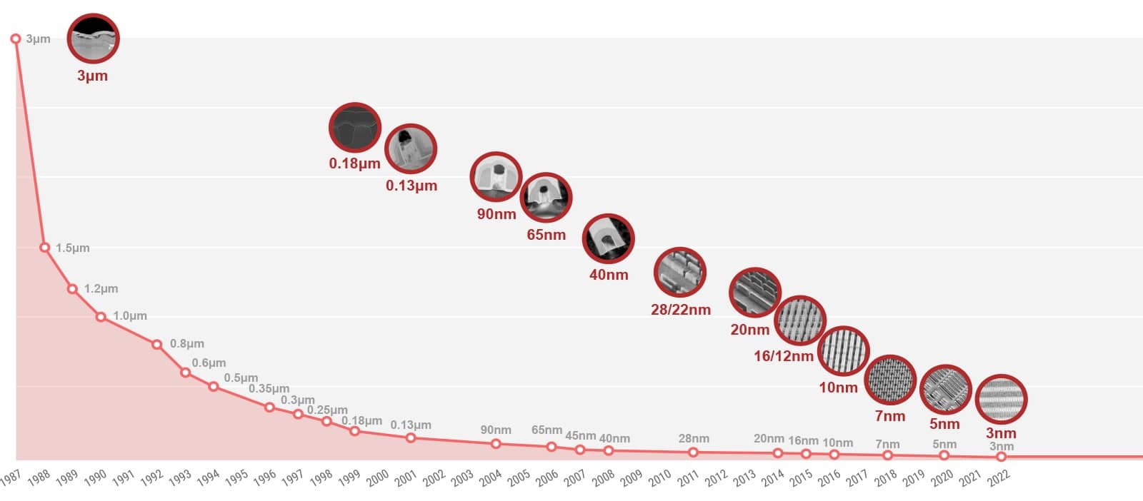
Since its founding in 1987, Taiwan Semiconductor Manufacturing Company (TSMC) has maintained a prominent position in the global semiconductor industry thanks to its strong internal research and development strategy. The company not only provides the most advanced foundry process technologies but has also achieved significant milestones at every stage of semiconductor evolution. Below is an overview of TSMC’s main logic technologies, from early advancements to the most modern nodes.
Recent Innovations: A16 and 2nm
- A16™ Technology
TSMC has introduced its A16™ technology, based on nanosheets and equipped with the innovative backend power delivery solution called Super Power Rail (SPR). This approach significantly enhances logic density, performance, and energy efficiency, laying the groundwork for future developments in high-tech nodes. - 2nm Node (N2)
Currently in advanced development, TSMC’s 2nm technology represents the company’s first generation of nanosheet transistors. This node offers significant improvements in performance, transistor density, and energy efficiency, marking a key step in the miniaturization of semiconductors.
Recent Production Technologies: 3nm and 5nm
- 3nm Node (N3)
In 2022, TSMC led the industry with mass production of 3nm FinFET technology. This node, considered the most advanced in the industry, is crucial for applications requiring high efficiency and transistor density, such as mobile devices and data centers. - 5nm Node (N5)
Introduced in 2020, this node enabled TSMC’s customers to develop innovative products with high performance and energy efficiency. N5 marked a milestone in the mass adoption of advanced technologies in key sectors.
Previous Advances: From 7nm to 0.13 Microns
- 7nm Node (N7)
Launched in 2018, the 7nm FinFET node was one of TSMC’s fastest and most successful developments, laying the foundation for the deployment of advanced technologies in the automotive industry, mobile devices, and more. - 0.13 Micron Node (µm)
In 2001, TSMC revolutionized the market with the launch of the first low-k copper process for systems on chip (SoCAn SoC, short for Security Operations Center (centro de…). This development improved efficiency and reduced power losses.
Pioneering Innovations: From 0.18 Microns to 3 Microns
- 0.18 Micron Node (µm)
In 1998, TSMC launched the first low-power 0.18 micron process, setting a standard for energy efficiency in industrial applications. - 3 Micron Node
From its inception, TSMC committed to an internal development strategy, starting with its 3 micron node. This node marked the beginning of a continuous evolution towards miniaturization.
TSMC’s Commitment to Innovation
TSMC’s technological history not only reflects continuous progress but also its ability to anticipate the demands of the global market. Each node represents a step forward in density, performance, and energy efficiency, facilitating significant advancements in areas such as artificial intelligence, the Internet of Things (IoT), high-performance computing, and more.
With technologies like the 2nm node and A16™ on the horizon, TSMC continues to lead the industry, setting new standards in semiconductor manufacturing and solidifying its role as a key player in global technological development.