
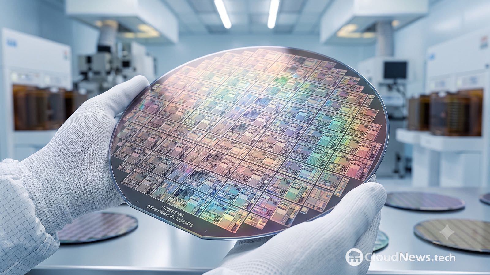
TSMC and a team of researchers from the National Yang Ming Chiao Tung University (NYCU) in Taiwan have demonstrated a new technique for manufacturing atomically thin monolayer molybdenum disulfide (MoS₂) transistors. This material is among those being explored by the industry to continue shrinking transistor sizes as traditional silicon approaches its physical limits. While this advance does not mean TSMC has a commercial less than 1 nanometer process ready, it addresses one of the key challenges to using 2D semiconductors in future chips.
The key points of TSMC’s future transistors in 20 seconds
- TSMC and NYCU have fabricated transistors using single-layer MoS₂ as the channel.
- The researchers introduce an ultra-thin layer of aluminum oxide just 0.42 nanometers thick.
- This interface facilitates the subsequent integration of hafnium oxide dielectric and reduces electron dispersion.
- The work is experimental and still far from a commercial node.
Published on July 31, 2026, in Nature Electronics, the study tackles an increasingly critical challenge in the semiconductor industry: continuing to shrink physical transistor dimensions while maintaining good current control, reasonable power consumption, and fabrication processes scalable to large wafers.
Why silicon is starting to need alternative materials
For decades, the industry has increased transistor density within chips by shrinking their sizes and progressively modifying their architectures.
Planar transistors gave way to FinFETs, where the channel takes a three-dimensional ‘fin-like’ shape. Later, Gate-All-Around FETs (GAAFETs) emerged, with gates that surround the channel even more completely to improve electrostatic control.
Problems arise when the thickness of this channel continues to decrease.
At extremely small scales, maintaining a sufficiently thin conventional semiconductor channel becomes challenging. Increased leakage, resistance, and difficulty in gate control of electron flow occur.
This is where so-called 2D materials come into play.
Molybdenum disulfide can form layers approximately 0.7 nanometers thick, nearly the thickness of just a few atoms. Unlike an extremely thin silicon sheet, it retains valuable semiconducting properties even when reduced to a single layer.
This makes it one of the most studied candidates for transistors beyond current GAAFET generations.
But having an ultra-thin channel solves only part of the problem.
A layer of just 0.42 nanometers makes a difference
To control the current passing through a transistor, there is a gate separated from the channel by an insulating layer called the gate dielectric.
This layer must be extremely thin to allow the electric field to effectively control the channel, yet it must also prevent direct current flow across the insulator.
High-permittivity or high-κ materials, such as hafnium oxide (HfO₂), have been used for years precisely to balance this requirement.
However, depositing these dielectrics directly onto MoS₂ proves challenging. The surface of 2D materials lacks the chemical bonds that usually facilitate uniform growth of deposited materials.
The researchers’ solution was to modify the interface first.
They deposited an ultra-thin layer of epitaxial aluminum on MoS₂ and then oxidized it to form about 0.42 nanometers of Al₂O₃ (aluminum oxide). On this surface, they then deposited the high-κ hafnium oxide dielectric.
This creates a sort of atomic bridge between the 2D semiconductor and the dielectric layer above.
This layer serves two functions: it provides a much more favorable surface for growing HfO₂ and reduces interactions that cause electron scattering in the channel.
This second effect is particularly valuable.
In an extremely small transistor, simply making it work isn’t enough. Electrons must traverse the channel with minimal resistance and scattering to achieve high performance at reasonable power consumption.
The transistor achieved high transconductance
Researchers fabricated top-gate transistors using monolayer MoS₂ obtained via chemical vapor deposition (CVD).
In devices with channels around 100 nanometers, they recorded a maximum transconductance close to 0.45 mS/µm, along with low leakage currents and minimal hysteresis.
Transconductance, in simplified terms, measures how much the transistor’s current can change with the applied gate voltage. A higher figure indicates effective gate control of the channel.
The significance of this work lies in achieving this behavior within an extraordinarily thin structure.
The authors argue that interface engineering can enable combining an extremely reduced equivalent dielectric with high carrier mobility—two objectives often in conflict in 2D transistors.
This doesn’t mean TSMC will manufacture 0.7 nm chips tomorrow
It’s important to distinguish between the physical dimensions used in research and the commercial naming of future process nodes.
Using a MoS₂ channel approximately 0.7 nanometers thick or an Al₂O₃ interface of 0.42 nm does not mean producing a processor with a “0.7 nm node”.
Current process names like 3 nm or 2 nm do not refer to a single physical dimension. Instead, they denote a set of improvements in density, performance, power consumption, and manufacturing technology.
Therefore, the work by TSMC and NYCU should be viewed as research into technologies that could enable future transistor generations when current architectures face scaling limitations.
It also does not yet mean fabricating billions of these devices with the performance, uniformity, and costs required for commercial processors.
Such a leap is typically much more complex than demonstrating an individual transistor or small array in a laboratory setting.
2D materials are beginning to approach industrial processes
What’s exciting is that this research is not isolated.
Throughout 2026, TSMC has also collaborated with imec and ASML on integration pathways for 300 mm wafers with transistors based on 2D materials, including MoS₂, WS₂, and WSe₂. According to TrendForce, these studies have demonstrated devices with a contacted poly pitch of 50 nm using processes designed to approach industrial-scale manufacturing.
Intel and imec are conducting similar research architectures.
This doesn’t guarantee that 2D materials will replace silicon. The industry has other options to increase density, such as new GAAFET structures, stacked transistors, 3D integration, advanced packaging, and novel power delivery techniques.
However, MoS₂ offers the ability to create a semi-conductor channel with an almost atomic thickness, which is particularly challenging with conventional materials.
The contribution of this new work is demonstrating how to build a high-quality gate interface around that channel without destroying its advantageous properties.
The race for future chips will depend not only on making structures smaller but also on controlling surfaces, contacts, and layers that are now being measured in atoms.
Frequently Asked Questions
What exactly have TSMC and NYCU achieved?
They demonstrated top-gate transistors with a monolayer MoS₂ channel using an aluminum oxide interface approximately 0.42 nm thick, enabling the integration of hafnium oxide dielectric while maintaining good electrical properties.
Does this mean TSMC can already produce sub-1 nm chips?
No. This is an experimental study on individual components of future transistors. The dimensions cited refer to specific physical layers and do not correspond to a commercial process node.
Why use MoS₂ instead of silicon?
MoS₂ can retain semiconductor properties in a layer about 0.7 nm thick, allowing for much thinner channels with effective electrostatic control.
When might this technology reach commercial processors?
The study doesn’t specify a timeline. Widespread adoption would require advances in large-scale manufacturing, uniformity, contacts, wafer performance, costs, and integration with existing processes.
via: wccftech
