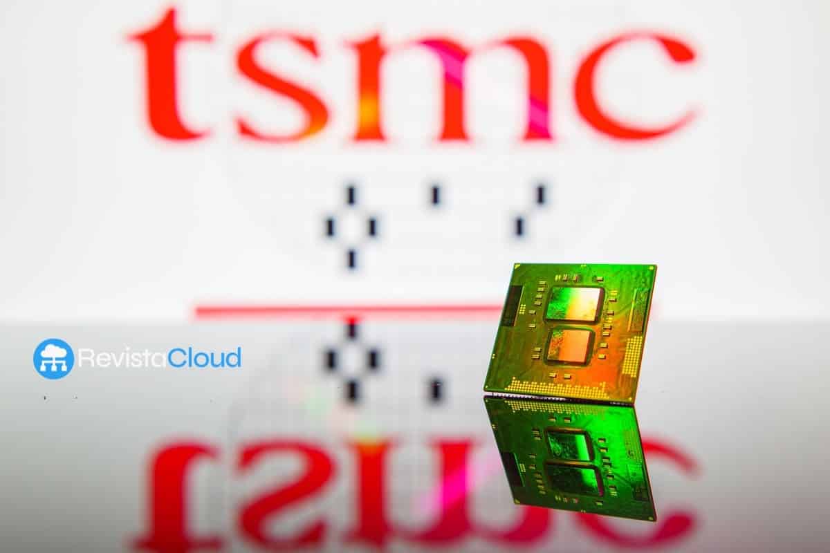
TSMC has leveraged its Open Innovation Platform Ecosystem Forum to send a very clear message to the entire industry: in high-performance computing and artificial intelligence, its strategy is based on three parallel pillars — advanced silicon, advanced stacking, and advanced packaging. This isn’t just marketing; behind it lies an aggressive roadmap with 2 nm nodes and beyond, new NanoFlex standard cells, and a packaging ecosystem already shaping the next generation of AI accelerators.
VSORA and its Jotunn 8: Europe’s showcase of the TSMC ecosystem
One example TSMC highlighted is VSORA, a French company that has relied on the foundry’s ecosystem to develop an AI accelerator based on RISC-V.
Its chip Jotunn 8 includes:
- 288 GB of HBM3E memory
- Memory bandwidth of 8 TB/s
- Two compute chiplets totaling 144 billion transistors
- 3.2 PFLOPS of dense FP8 compute power
The compute chiplets are fabricated on TSMC’s N5 node and assembled using CoWoS-S packaging inside a package roughly 70 × 80 mm. According to VSORA, the development process took about 18 months, a tight timeline for such a complex design, demonstrating how mature the TSMC-based design ecosystem (EDA, IP, packaging) is for next-gen AI products.
From N3 to N2, A16, and A14: the race beyond 2 nm
On the silicon front, TSMC is transitioning from the N3 (FinFET) family toward 2 nm (N2), where the nanosheet (gate-all-around) transistor architecture finally comes into play.

The company maps out its roadmap as follows:
- N2: now ramping to volume production for leading HPC and mobile customers. Early designs show performance gains of around 16% at the same power and energy savings of over 30% compared to N3E, depending on the core and library used.
- N2P: an optimized evolution of N2 planned for early 2026, with further improvements in performance and efficiency.
- A16: a new node combining nanosheet transistors with backside power delivery (BSP), internally named Super Power Rail (SPR), with initial chips expected by late 2026.
- A14: the next step after A16, featuring an improved nanosheet design and further enhancements in performance per watt.
TSMC estimates up to 1.8× performance improvement at the same power when comparing the full jump from N7 to A14, and approximately 4.2× efficiency gains in the same transition. Between N2 and A14, the foundry anticipates frequency increases around 16% at constant power or power reductions at the same performance.
In the nearer term, the A16 with SPR node should deliver 8–10% higher frequency at the same voltage compared to N2P, or alternatively a 15–20% power reduction while maintaining performance, according to TSMC’s internal data shared with clients.
NanoFlex: custom standard cells for design flexibility
A key technical innovation is the introduction of NanoFlex alongside the N2 family. NanoFlex enables mixing and matching different types of standard cells within the same design — wider and faster for critical paths, more compact and efficient for less demanding logic — without penalizing the design flow.
According to TSMC, this approach can yield chips that are up to 15% faster or 30% more efficient simply by selecting the appropriate library combination within the same node.
In essence, it’s not just about the node itself but also the full kit — libraries, design rules, and tools provided by TSMC — to maximize the node’s capabilities in different directions: performance, power efficiency, or area density.
Backside power delivery: from N2P to A16
An important aspect of the roadmap is the strategic move toward backside power delivery. Initially, TSMC associated backside power with N2P, but recent updates move this innovation to A16, making it the de facto node where nanosheets and backside power converge within the 2 nm platform.
Backside power reduces front-side area dedicated to transistors by relocating power lines to the wafer’s backside. This lowers resistance and inductance in the supply network, facilitates higher frequencies, and enables denser and more modular chip architectures.
Advanced packaging and stacking: CoWoS, HBM, and 3D as standard
Beyond silicon, TSMC emphasizes that having the “best node” isn’t enough: current AI and HPC designs rely heavily on advanced packaging that combines multiple compute chiplets with stacked HBM memory in a single system.
The company leads in this area with its 3DFabric technologies, which include:
- CoWoS (Chip-on-Wafer-on-Substrate), with variants like CoWoS-S, used in VSORA’s Jotunn 8, and in many top-tier AI GPUs.
- SoIC and other 3D stacking solutions for integrating logic and memory dies with very high-density interconnects.
- Advanced packaging designed specifically for multi-terabyte-per-second bandwidths and multi-hundred-watt power consumption.
This means TSMC not only fabricates chips but also provides an integrated path from tape-out to fully assembled modules with HBM, interposers, and substrates ready for server deployment.
AI at the manufacturing level
The company also highlighted that AI plays an internal role in its processes: from logical design and verification, through layout optimization, to manufacturing control and testing.
Many of these techniques have been grouped under machine learning for years, but the increasing complexity of 3 nm and 2 nm nodes has made these models essential tools for maintaining performance, yield, and quality within acceptable parameters.
“No path around TSMC” in HPC and AI
Overall, the message from the forum is clear: in the coming years, no high-performance and AI chip designer without a foundry partnership will be able to ignore TSMC if they want to stay at the forefront of technology.
The foundry not only offers the most advanced nodes in the market but also:
- Integrates early-stage collaboration with leading EDA tools.
- Provides libraries and technologies like NanoFlex to maximize 2 nm and subsequent nodes.
- Leads in advanced packaging necessary for large-scale chiplet and HBM integration.
- Aligns its roadmap with the evolving needs for training and inference of ever-larger AI models.
While Intel and Samsung Foundry aim to catch up in nodes and packaging, TSMC has positioned itself as controlling silicon, stacking, and packaging for the next wave of AI hardware. All signs point to this combined leadership shaping industry standards over the next decade.
via: hardwareluxx