The Taiwanese TSMC has made it clear that its commitment to the United States is no longer a test but an industrial-scale project. During the third-quarter earnings presentation, CEO C. C. Wei confirmed two major moves: the acquisition of a second site near its Arizona facilities to expand capacity and the accelerated update of its technological roadmap to bring the N2 (2 nm) node and “beyond” processes to the Sonora desert. According to the executive, this responds to a “very strong multi-year demand related to AI” from U.S. customers.
“We are making tangible progress and executing our plan well. Additionally, we are preparing to fast-track our technology updates to N2 and advanced processes in Arizona, driven by the strong AI-related demand from our customers,” Wei said. “We’re close to securing a second large plot nearby to support current expansion and provide us flexibility to meet this demand.”
Currently, the TSMC Arizona complex produces in 4 nm, but the company’s goal is to close the temporal gap with Taiwan and bring the most advanced nodes closer to the U.S. If the schedule holds, TSMC would become, after Intel, the second manufacturer to introduce 2 nm in the U.S., possibly as early as the second half of 2026. The company has also hinted at future plans to scale in Arizona to A16 (1.6 nm), driven by the significance of its U.S. customers—NVIDIA, AMD, Apple—in its financial results.
Why TSMC is Accelerating in the United States
The short answer is AI. The wave of accelerators for training and inference has skyrocketed demand for advanced wafers (N5/N4 today, N3/N2 tomorrow), and big tech—from GPU designers to SoC developers—want to manufacture part of their volume in America. For TSMC, relocating part of its leading-edge pipeline to Arizona is both a business opportunity and a strategic decision: it diversifies geography, brings production closer to customers, and aligns with the “Made in USA” narrative without sacrificing its leadership position in Taiwan.
From an American perspective, this move broadens the local supply of advanced semiconductors. Until now, Intel led the race for 2 nm (its 20A/18A nodes served as a bridge to what the market perceives as the “sub-2 nm era”), but with TSMC joining in, the market will see two providers capable of serving 2 nm nodes within 12–24 months. This duopoly for leading-edge processes adds redundancy, a strategic advantage that customers, regulators, and markets interpret as a move toward a more resilient supply chain.
What Does N2 (2 nm) Mean for AI Customers?
The node shrink—from 4 nm in production today to 2 nm in the plan—is not cosmetic. It brings higher logic density, better performance per watt, and the ability to assemble more ambitious chiplets with high-speed interconnects. For GPU and AI accelerators, each performance/efficiency improvement allows for more compute per rack, reduces energy costs, and improves latencies. For client CPUs and SoCs, 2 nm opens doors to more capable integrated NPUs and longer-lasting batteries without sacrificing performance.
Moreover, bringing N2 to Arizona reduces logistics and simplifies certification for clients who need to assemble, test, and deliver in America: less international transit, shorter timelines, and faster response to demand spikes.
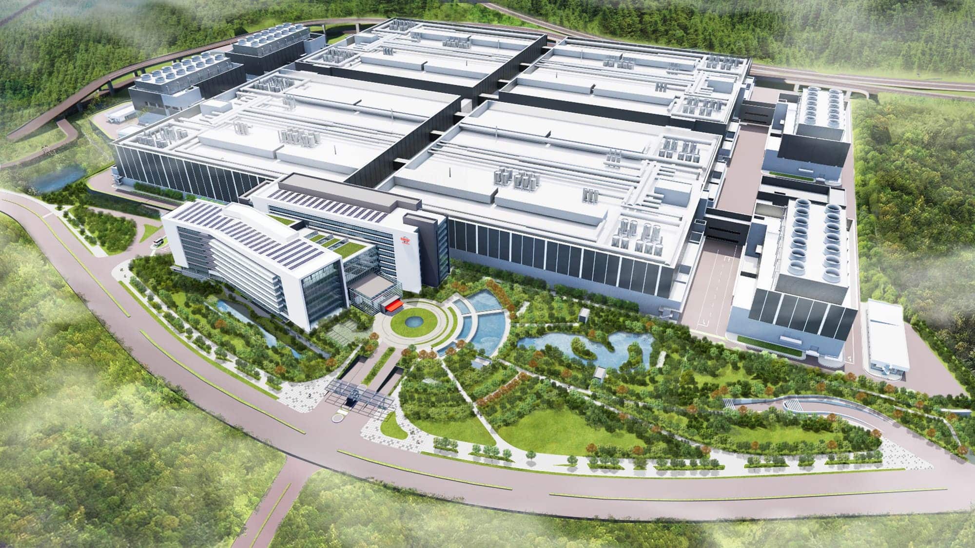
Second Site in Arizona: More Facilities, Greater Flexibility
The announcement of a second site near current facilities goes beyond “growth for growth’s sake.” TSMC is seeking flexibility to modulate expansion depending on the multi-year AI demand. The company already operates six fabs on the complex and plans to expand with new units for next-generation processes. This land buffer allows planning photolithography, clean rooms, and backend to match actual market demand, avoiding overcapacity or bottlenecks.
The Taiwan–U.S. Gap and How it Is Closing
For years, TSMC’s cutting edge manufacturing took place exclusively in Taiwan. Bringing N2 to the U.S. won’t immediately erase that temporary advantage of the island (Taiwan will remain 1–2 years ahead in subsequent nodes), but it closes the gap. In practice, U.S. customers will see earlier in Arizona the nodes that currently travel from Hsinchu, with a reduction of the lead time that C. C. Wei has acknowledged as a goal.
In the medium term, the plan extends further: A16 (1.6 nm) in Arizona is on TSMC’s horizon, signaling that the East-West transition in advanced processes won’t be just a momentary shift but an ongoing trend.
Operational Risks and the Ultimate Test
The move from 4 nm to 2 nm involves more than additional EUV: it requires talent pipelines, chemical suppliers, photo masks, testing equipment, and auxiliary services that are established in the region. TSMC has shown it can build fabs—despite learning curves and cost overruns—but scaling N2 in Arizona will be a true test: performance, yield, and quality must match what is already achieved in Taiwan.
Additionally, synchronization with key anchor customers (such as NVIDIA, AMD, Apple) will be crucial. For N2 “to be worthwhile” in Arizona, the demand, design readiness, and installed capacity must align.
Schedule and Key Indicators to Watch
- N2 in Arizona: TSMC aims to launch 2 nm in the U.S. by H2 2026.
- A16 (1.6 nm): explicit plan to scale in Arizona to A16 after N2, with specific timeframes to be determined.
- Second site: completion of second land purchase and expansion project.
- Customer mix: public announcements of wafer starts for GPU/CPU/SoC with N2 in the U.S.
- Hiring and ecosystem development: agreements with local suppliers, training, and team relocations involving EUV process experience.
What Benefits Does the U.S. Ecosystem Gain?
For the U.S. semiconductor supply chain, the deployment of N2 and later A16 signifies a maturing of the entire ecosystem: from gases and chemicals to metrology, bonding, probing, packaging, and testing. It also aligns public incentives—federal and state—with high-impact projects and skilled employment. Additionally, it reduces the geographical monopoly of leading-edge processes, a strategic priority pursued for years.
The Core Driver: AI as the Demand Engine
The common thread through all these announcements is AI. Without the appetite for GPU and accelerator chips—and integrated NPU-based SoCs—moving to N2 in Arizona would be slower. TSMC acknowledges that orders from NVIDIA, AMD, and Apple are driving the push for technological upgrades and capacity. If current demand trends continue, the process gap between the U.S. and Taiwan at critical AI nodes will narrow.
Frequently Asked Questions
When will TSMC start manufacturing 2 nm (N2) chips in the U.S.?
TSMC has indicated its intention to bring N2 to Arizona and begin production as early as H2 2026, accelerating the move from the current 4 nm.
Why is TSMC purchasing a second site in Arizona?
To expand its campus and gain flexibility. The company is close to completing the second land acquisition, which will enable new fabs and additional space for N2 and future nodes.
Who are the main customers driving this expansion and what do they want?
Demand comes from NVIDIA, AMD, Apple, and others, primarily focusing on AI. They seek local capacity for leading-edge nodes and predictable timelines; TSMC is responding by bringing N2 closer to the U.S. and planning for A16 (1.6 nm) later on.
What does “A16 (1.6 nm)” mean in TSMC’s roadmap?
It’s the commercial name for an advanced node (around 1.6 nm in marketing taxonomy). TSMC intends to scale in Arizona to A16 after N2, establishing cutting-edge production in the country.
What is TSMC currently producing in Arizona, and why is moving to N2 important?
Today, the site manufactures 4 nm. Transitioning to 2 nm means better performance/per watt for GPUs, CPUs, and SoCs, increased density, and a competitive edge for AI customers seeking local manufacturing and shorter lead times.