In the race for AI chips, the focus is often on large factories and next-generation nodes. But there is a less visible—yet critical—reality: without the machines that enable depositing, etching, and structuring materials at the nanometer scale, the accelerators that today support data centers, high-performance computing, and even gaming would not exist.
This is the arena where Lam Research plays, one of the most important suppliers of equipment for semiconductor manufacturing. The company, headquartered in Fremont (California) and traded on Nasdaq under the ticker LRCX, designs and manufactures tools used by leading chipmakers for critical wafer processes such as deposition of thin films, etching, cleaning, and photoresist removal, among others. In other words: Lam doesn’t sell “chips,” but the industrial technology that makes building them with precision and repeatability at scale possible.
From this perspective, it’s clear why an apparently “industrial” announcement—a US-based manufacturing of a new piece of equipment—has strategic significance. Lam has its focus on its Tualatin (Oregon) campus, in the Portland metropolitan area, where its newly launched VECTOR® TEOS 3D deposition system is assembled and validated. This system is designed to address bottlenecks in advanced packaging, an increasingly critical discipline for 3D chips used in AI and HPC.
VECTOR® TEOS 3D: when packaging becomes the new battleground
Advanced packaging is no longer a “minor final step.” The industry is stacking chiplets, increasing density, and using complex interconnections to boost performance without relying solely on shrinking transistors. In this landscape, Lam positions VECTOR® TEOS 3D as a tool aimed at a specific problem: filling gaps between dies and 3D structures with thick dielectric films, avoiding defects and maintaining uniformity on wafers that may present challenging curvatures.
The company describes the system as capable of delivering “ultra-thick” gapfill dielectric films of up to 60 micrometers, emphasizing its focus on integration challenges from stacking dies, especially in wafers with “high bow” (curvature). Practically speaking, this is another piece within an industrial trend: as chips become three-dimensional, manufacturing requires more specialized tools.
Lam frames the launch as part of its portfolio of “made in USA” tools for global customers. It also highlights other platforms produced in the US, such as Flex®, Kiyo®, and SABRE® 3D, which are linked to different stages of the manufacturing process.
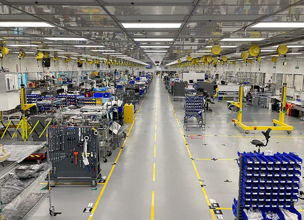
A workshop that doesn’t operate like a “production line”
One of the key points Lam emphasizes from Tualatin is that the manufacturing environment is far removed from the typical image of a linear assembly line. The plant is organized with two teams working literally “around the corner”: Pilot Engineering and Manufacturing/Assembly. This physical proximity is not just a detail—it enables process design, assembly flow, and troubleshooting to occur almost in real time.
The Pilot Engineering team—explains the company—defines how the tool is assembled throughout the plant, optimizes the design with the product team, and establishes testing procedures to validate the system before it ships to customers. On the manufacturing side, the operational goal is described with a very “high-tech factory” phrase: “strike plasma,” energize the system, and ensure it is ready to operate before shipping.
This rapid coordination, free from internal bureaucracy or weeks of departmental delays, is especially valuable when launching a new product line and the industrial process is still being refined.
Local talent, technical training, and multidisciplinary teams
Lam also highlights its Tualatin workforce, stating that the plant employs people from diverse backgrounds and sources a significant portion of its staff from the local educational ecosystem: from Portland Community College and Clackamas Community College to Oregon State University, Oregon Institute of Technology, and Portland State University, among others in the region.
The team includes manufacturing, electrical, mechanical, industrial, and software engineers alongside prototyping technicians, troubleshooting specialists, and test personnel. The message is clear: in advanced manufacturing, simply “screwing in bolts” isn’t enough—cross-disciplinary skills and continuous learning are required because the product and process evolve simultaneously.
Safety and retention: an underappreciated competitive advantage
Another point Lam stresses is safety as a central part of its manufacturing culture. The company states that its Tualatin site has been recognized under OSHA’s Voluntary Protection Program (VPP), which honors organizations with effective safety and health systems and incident rates below industry averages. Lam adds that the campus is the largest employer in Oregon with this recognition and has ranked second nationwide at times.
In addition to this safety culture, the company implements concrete measures: optimized work practices to minimize risks, tools and fixtures to reduce hazards at the workstation, and an ergonomics team providing physical therapy support for employees.
The core message is that in a sector with fierce talent competition, retention is just as important as machinery. In facilities where precision and accumulated knowledge are crucial, losing experienced personnel means losing industrial advantage.
What is Lam Research and why does it matter in the global chip supply chain
To understand the significance of this news, it’s helpful to clarify what Lam does in the market. Lam Research is a global provider of wafer fabrication equipment and related services, used by semiconductor manufacturers to build transistors, interconnections, advanced memories, and packaging structures. Its role is that of a technological enabler: as the industry transitions to new architectures (3D, chiplets, HBM, gate-all-around nodes), it needs tools capable of maintaining performance and reliability at scale. This is where companies like Lam become the invisible infrastructure supporting the AI boom.
With VECTOR® TEOS 3D manufactured in Oregon, Lam also bolsters an industrial argument gaining weight in the US: the ability to produce critical technology locally with qualified domestic capacity, reducing reliance on external supply chains. Simultaneously, it sends a message to its clients: advanced packaging is no longer just a “complement,” but the new frontier that will determine who leads the next generation of chips.
Frequently Asked Questions (FAQ)
What is the purpose of a deposition tool like VECTOR® TEOS 3D in advanced packaging?
It is used for depositing dielectric films employed in 3D integration and die stacking processes, helping to address fill (gapfill) and reliability challenges in advanced chips for AI and high-performance computing.
Why is gapfill between dies so important in 3D chips for AI?
Because stacking and high density require filling spaces uniformly and defect-free: any void or variation can impact performance, thermal stability, and electrical reliability of the package.
What is the difference between deposition, etching, and cleaning in semiconductor manufacturing?
Deposition adds material layers; etching removes material to define structures; cleaning and stripping eliminate residues and photoresist. These are sequential, critical steps—failure in any compromises the chip’s compliance with specifications.
What is OSHA’s VPP program, and why is it mentioned in a high-tech plant?
It’s a voluntary program recognizing advanced safety and health systems. In complex factories, a strong safety culture can enhance retention, operational quality, and continuous production.
via: newsroom.lamresearch