
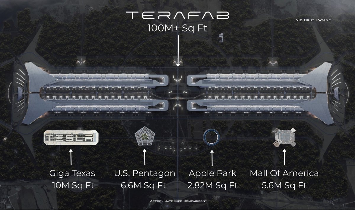
Elon Musk wants his future semiconductor plant, Terafab, to let Tesla and SpaceX design, manufacture, and test around ten chip designs a year. The idea is to shorten development cycles and reduce dependence on outside manufacturers like TSMC, but the target refers to experimenting with new designs, not mass-producing ten commercial chips every year. The challenge is turning that development speed into competitive industrial capacity, which requires far more than a fab and AI-assisted design tools.
Terafab’s key facts and its chip-manufacturing goal, in 20 seconds
- Musk proposed manufacturing and testing around ten chip designs a year at a research fab located at Giga Texas.
- The goal is to speed up the cycle between design, manufacturing, testing, and new revisions.
- Terafab aims to supply the needs of Tesla, SpaceX, and their artificial intelligence (AI) projects.
- Intel has joined the project, and Tesla has pointed to Intel’s 14A manufacturing process as a technology option.
- Competing with TSMC at scale will require mastering manufacturing yield, costs, production, and advanced packaging.
The initiative is part of Musk’s plan to control a larger share of his companies’ chip supply chain. Tesla needs processors for its vehicles, self-driving systems, and Optimus robots, while SpaceX and xAI require compute capacity for their artificial intelligence projects. Terafab’s strategy aims to bring design and manufacturing closer to the needs of those products.
During a meeting with Tesla owners and investors held on October 11 in Austin, Texas, Musk admitted he doesn’t know how to manufacture chips and argued for the need to learn through experimentation. His proposal is to create an environment where teams can test designs far more often than in conventional processes.
The distinction matters: the initial goal isn’t to produce ten ready-to-sell commercial generations, but to achieve ten designs that can be manufactured and evaluated within a year. Some might not work, and others would need changes before reaching stable production.
A Research Fab to Speed Up Chip Development
Terafab’s first phase involves a research fab on the Giga Texas campus in Austin. According to information published by Reuters in May 2026, Musk estimated this facility could cost around $3 billion and process a few thousand wafers a month. Its main role would be to test ideas and designs, not to compete with major commercial fabs from day one.
The overall plan is more ambitious. Musk has described two main manufacturing tracks: one for Tesla vehicle and humanoid robot chips, and another for the AI data centers tied to his space projects. The final scale, launch dates, and part of the industrial structure are still to be worked out.
In this scenario, the goal of ten designs a year makes sense as a research strategy. Development teams need to see how a real chip behaves, catch errors, and adjust the design. A simulation can anticipate many problems, but it doesn’t replace all the physical testing that manufactured silicon requires.
Each manufacturing cycle provides information about power consumption, performance, stability, and thermal behavior. If the fab allows these tests to be repeated more often, engineers could catch failures earlier and discard designs that don’t meet requirements.
Artificial intelligence can also speed up some design, verification, and analysis tasks. However, physical manufacturing still depends on specialized equipment, materials, lithography processes, and numerous industrial steps. Cutting the time needed to prepare a design doesn’t automatically eliminate the weeks or months it can take to produce, measure, and validate a chip.
That’s why the research fab’s success will depend on how much it manages to shorten the full cycle, from design to test results. Ten designs started on paper aren’t the same as ten working chips, let alone ten products ready for mass production.
What Terafab Needs to Compete With TSMC
TSMC, short for Taiwan Semiconductor Manufacturing Company, is one of the world’s leading independent semiconductor manufacturers. Its advantage isn’t limited to having advanced fabs: it also has decades of experience in manufacturing processes, quality control, wafer yield, supplier relationships, and production for large customers.
Terafab starts from a different position. Its immediate goal is to develop capacity for the needs of Musk’s companies, not necessarily to build a business that manufactures chips for a broad portfolio of external customers. That difference can simplify some design decisions, but it also limits the demand diversification that helps sustain large-scale industrial investments.
Reuters reported in May that SpaceX had floated an initial investment of $55 billion for a semiconductor manufacturing facility in Texas. The same report included an estimate of up to $119 billion for the entire project if additional phases are completed. These are figures tied to announced plans, not confirmation that the full investment has been carried out.
Manufacturing technology is another key factor. Musk has said Tesla intends to use Intel’s 14A process once Terafab reaches a more advanced stage. Intel joined the project in April 2026, bringing industrial expertise. Still, a technological intention doesn’t prove the fab already has the equipment, validated processes, or capacity needed to produce chips at volume.
Beyond manufacturing the silicon itself, Terafab would also need to handle advanced packaging, final testing, and integrating the chips into complete systems. In AI accelerators, processor performance also depends on memory, internal interconnects, power delivery, and cooling.
The comparison with TSMC needs to account for all of these elements. A research fab can become a valuable tool for speeding up the development of in-house designs without coming close to matching one of the industry’s largest manufacturers in capacity, cost per chip, or process variety.
The Advantage Might Be Learning Faster, Not Manufacturing More
Musk’s approach echoes a common strategy in complex product development: increasing test frequency to catch errors earlier and lower the cost of each attempt. For chips, the value of that approach depends on whether new versions can be manufactured at an affordable cost and whether the results translate into concrete improvements.
An in-house facility could also give Tesla and SpaceX more control over development timelines. Instead of depending entirely on an external manufacturer’s available capacity, their teams could better align testing with their products’ needs. That doesn’t mean they’ll stop relying on specialized suppliers, especially while Terafab is still in its early stages.
Semiconductor manufacturing demands extreme industrial precision. Production yields, process stability, and the ability to manufacture millions of units with consistent characteristics matter just as much as the speed at which a new chip is designed. A facility capable of producing prototypes quickly can add value, but it still has to prove it can carry those results over into commercial manufacturing.
Reuters’ own reporting warns that Terafab’s timeline and several aspects of its execution remain unresolved. The scale of investment, supplier selection, and the facilities’ launch are all still open questions, so there isn’t yet enough basis to claim the project will match TSMC.
The goal of ten designs a year will matter if it lets Musk’s teams learn faster and develop processors better suited to their vehicles, robots, and AI systems. The real test will come when Terafab can show not just that it can produce prototypes, but that it manufactures working chips with strong performance, competitive costs, and enough capacity to meet expected demand.
Frequently Asked Questions
What is Terafab?
Terafab is the semiconductor manufacturing project driven by Elon Musk’s companies to develop chips for vehicles, robots, and artificial intelligence systems. The initiative includes a research fab and later plans for larger-scale facilities in Texas.
What does manufacturing ten chip designs a year mean?
It means trying to design, manufacture, and test around ten different designs over a year. It doesn’t mean all of them will work or that ten commercial chips will be produced in large quantities.
Can Terafab compete with TSMC?
There isn’t enough evidence yet to say so. Terafab needs to show it can manufacture chips with competitive performance, quality, costs, and industrial capacity.
What role will Intel play in Terafab?
Intel joined the project in April 2026, and Tesla has pointed to the 14A manufacturing process as an option for Terafab’s chips. The details of execution and timeline are still to be worked out.
