The United States is preparing a technological offensive at the heart of the semiconductor ecosystem: lithography. The emerging Substrate has introduced a proposal that combines particle accelerators with a X-ray source to print transistor patterns with a resolution that, according to the company, matches or exceeds that of the latest-generation EUV systems, but with less complexity and drastically lower costs. The goal is clear: reduce dependence on Europe — where ASML dominates EUV lithography — and Asia, and relocate the most critical piece of advanced manufacturing back to the U.S.
This is not an incremental bet; it’s a disruptive one: replacing the extreme ultraviolet (EUV) light with X-rays generated from electrons accelerated almost to the speed of light and then “shaken” by magnetic fields to emit extremely bright pulses. With this source, along with its own optical and mechanical system, Substrate claims to have printed arrays of contacts with critical dimensions of 12 nm and pitch-to-pitch spacing of 13 nm, as well as random vias with center-to-center spacing of 30 nm with high fidelity. As a qualitative reference, the company asserts that its results are equivalent to a 2 nm node in terms of resolution, with room to go “beyond.”
How it works: from the accelerator to the wafer
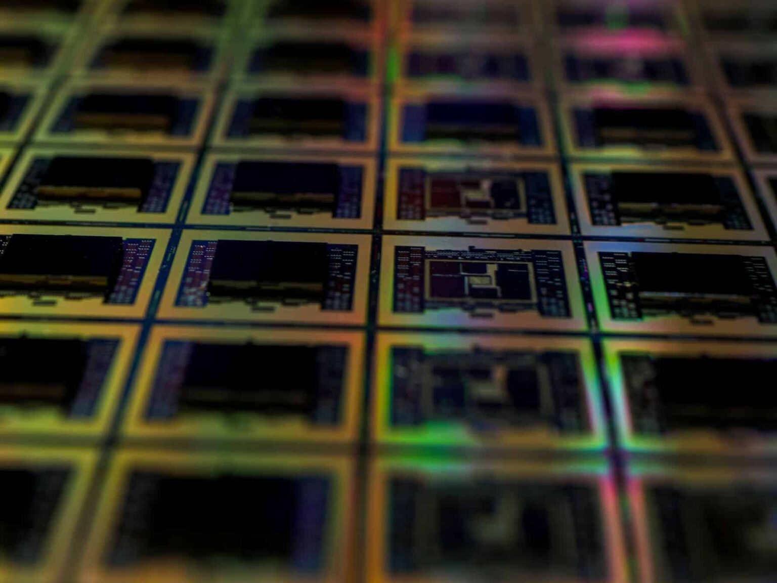
The core of the system begins with radiofrequency cavities that accelerate electron packets. These electrons, already highly energetic, pass through a sequence of alternating magnets (undulators and related devices) that trigger X-ray emission in intense pulses. The light is transported and shaped using a system of “polished-to-the-limit” optics until reaching the 300 mm wafer, where a high-acceleration mechanical module (with elevated G-forces) provides the scanning performance required for a cutting-edge factory. Substrate reports having built its first “production” lithography tool for 300 mm wafers, assembled internally.
The dual promise is: first, resolution: working with shorter wavelengths than EUV, printed structures could be finer, with fewer demands on extreme projection optics. Second, economies and timelines: by eliminating or simplifying highly complex and costly optical blocks of the current EUV ecosystem, and by verticalizing its chain (source + optics + mechanical), Substrate aims to reduce deployment times and overall costs.
Strategic angle: independence and cost per wafer
The broader message goes beyond physics. Substrate aligns its plan with America’s industrial autonomy: to regain leadership not only in design (where tech giants already excel) but also in manufacturing equipment and foundries. The company argues that the sector is heading toward unsustainable costs: factories exceeding $50 billion and wafers costing $100,000 by 2030, which would limit access to cutting-edge silicon to only a few corporations. In contrast, Substrate promotes a route to produce wafers for $10,000 “by the end of the decade,” an order of magnitude less than the current trajectory.
This reduction, if realized, would be seismic. It would transform the business model of the entire ecosystem: from chip design — increasingly assisted and automated by AI, according to Substrate — to the data economy, with more players capable of affording custom silicon. The bottleneck would shift from design (cost-effective via AI) back to manufacturing; precisely where the company intends to establish its advantage.
Direct hit to Europe (ASML) and a challenge to China
The move is also geopolitical. ASML, based in the Netherlands, holds the global monopoly on EUV and is effectively the gatekeeper to cutting-edge silicon. China, on its part, is heavily investing in domestic tools — including lithography — with the aim of becoming self-sufficient across the entire stack. Substrate argues that if the U.S. doesn’t accelerate, China could achieve self-sufficiency in most manufacturing tools — including advanced lithography — before 2030.
In that context, X-ray lithography based on accelerators aims to skip steps: not to compete directly with ASML’s high-NA, extreme optics EUV, but to redefine the architecture of equipment and significantly lower its construction, operation, and maintenance costs. The reduced dependence on critical optics and external components would be an advantage in today’s highly concentrated supply chain.
What remains to be demonstrated?
Technical skepticism, understandable, will undoubtedly remain. X-ray lithography is not a new concept: there were significant programs decades ago that failed due to complex and fragile masks, alignment/proximity issues, and, most importantly, productivity (throughput) and cost. While Substrate claims to have redesigned the stack — source, optics, mechanics — with a focus on high-volume manufacturing, the true challenge lies in:
- Real throughput (wafers per hour) with complex patterns and strict overlay requirements between layers.
- Resists that withstand doses and partial doses without blurring or chain degradation.
- Masks and a metrology chain with tolerances compatible with nodes <2 nm.
- 24/7 reliability in manufacturing environments, with predictive maintenance and competitive MTBF/MTTR.
- Process ecosystem (deposition, etching, CMP) calibrated to the profiles generated by the new exposure method.
None of these challenges are minor. Current EUV systems are engineering marvels built from decades of iteration with materials suppliers, optics, sources, masks, and metrology. Overcoming them requires public data, timelines, and pilot customers to validate performance and costs.
What is already on the table
Apart from the vision, Substrate lists milestones: an internal tool for 300 mm wafers operational, patterns with 12 nm CD / 13 nm tip-to-tip consistent with uniform quality, vias with a pitch of 30 nm of high fidelity, and a mechanical system capable of operating at high Gs to match the performance of a leading scanner. The company also states it is vertically integrated across its chain — optics, chemistry, metal mechanics — and has accelerated R&D using GPUs/TPUs and digital twins to compress multi-year iterations into days.
The roadmap aims to integrate this technology into new factories in the U.S., with compact modules and shorter deployment timelines than competitors. Its clear narrative: billions of wafers annually and a comprehensive American stack for future “AI factories.”
Implications if the bet succeeds
- Costs: if the cost per wafer approaches $10,000, it would democratize access to cutting-edge silicon and open new niches for specialized designs that are currently unfeasible.
- Capacity: smaller, cheaper equipment could multiply installed capacity without concentrating everything in a few mega-factories.
- Competition: while ASML would maintain EUV dominance, a rival with an orthogonal approach would emerge; China’s plans could be thwarted if the U.S. manages to industrialize the new process first.
- Risks: transitioning from prototype to high-volume manufacturing (HVM) remains the critical stage where many technological promises fail; sustained quality and mask economy will be decisive.
- Value chain: materials, resists, metrology, and EDA tools might require adjustments to optimize for X-ray exposure characteristics.
What about Europe?
For Europe, ASML is one of its most strategic assets and a unique case of global leadership in advanced hardware. A viable U.S. competitor would not only redistribute market power but also reopen debates on technological sovereignty and public support for R&D in manufacturing equipment. European foundries — and U.S. ones too — will closely evaluate the true TCO of Substrate’s tool: purchase price, operational costs, yield, and mask-to-product cycle.
Signals to watch in the next 12–24 months
- Technical publications with verifiable metrics (overlay, LER/LWR, CDU, MEEF) and process conditions.
- Pilot customers (logic, memory, or photonics) and installation sites with defined ramp-up windows.
- Mask and resist supply chains adapted to X-ray with stable supply.
- Throughput roadmap (wafers/hour) and cost per step comparable to high-NA EUV systems.
- Investment commitments (CapEx) and partnerships with equipment and process chemical suppliers.
The history of lithography is filled with brilliant ideas that failed to survive the harsh manufacturing reality. But it’s also true that the sector rewards jumps that reduce complexity and cost without sacrificing performance. If Substrate can sustain its promises with data, the U.S. would craft a new chapter in chip manufacturing… and Europe and China would need to recalibrate their strategies.
Frequently Asked Questions
How does Substrate’s X-ray lithography differ from ASML’s EUV?
EUV produces extreme ultraviolet light using CO₂ lasers that vaporize tin; this light is projected with extremely complex reflective optics. Substrate proposes X-rays generated with particle accelerators and a different optical and mechanical train. In theory, the shorter wavelength allows for greater resolution with less extreme optics.
Can this technology scale to industrial (HVM) levels?
That’s the big question. It must demonstrate throughput, layer overlay, suitable resists, robust masks, and 24/7 reliability. The shift from laboratory to volume manufacturing is where many alternatives have historically failed.
What impact could this have on chip costs?
Substrate claims it could reduce the wafer cost to around $10,000 “by the end of the decade,” compared to trajectories heading toward $100,000. If confirmed, it would make cutting-edge silicon more affordable and open the door to more customized designs.
How does this fit into the US–China rivalry and Europe’s role?
If the U.S. manages to industrialize a viable alternative lithography, it would diversify its dependence on critical equipment and reconfigure the balance with China — which aims for total autonomy — and with Europe, whose leadership in lithography (ASML) would be challenged for the first time in decades.
via: Substrate