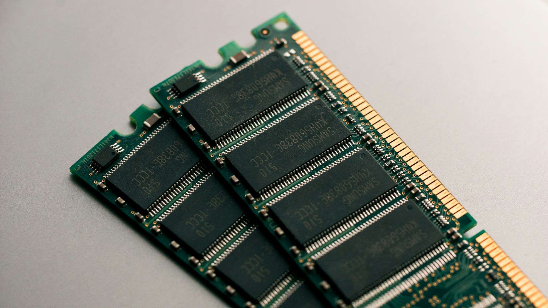
The South Korean Prosecutor’s Office has opened one of the most sensitive cases in recent years in the global battle over semiconductor technology. Ten individuals — including former Samsung Electronics employees — have been charged with leaking key information related to the manufacturing process of “10-nanometer” DRAM to ChangXin Memory Technologies (CXMT), a Chinese memory manufacturer. This technology is considered strategic and protected by the South Korean government.
According to the investigation, the incident involves the second generation of the 10-nanometer node in DRAM, known in the industry as “1y nm”. This miniaturization leap is not just about making smaller chips: it involves mastering hundreds of fabrication steps, fine-tuning process flows, and engineering decisions that, in practice, distinguish a promising prototype from a profitable mass production.
An ex-executive and a pattern: recruitment, manual copying, and development in China
The accusation centers around a figure identified as A, a former Samsung employee who, at CXMT, was responsible for leading the development of 10-nanometer DRAM. The Prosecutor’s Office claims that A and four other key development team members have been indicted and detained, while five area managers have been charged without detention.
The investigators describe a pattern combining talent acquisition, planning, and extraction of critical information. According to the Prosecutor’s Office, CXMT — a company backed by over 2.6 trillion won in local Chinese public investment — allegedly exploited the hiring of personnel with internal knowledge to accelerate the development of an advanced process, purportedly using South Korean technology unlawfully.
At the heart of the case is also a former researcher identified as B, accused of copying and leaking information about “hundreds of stages” in the 10-nanometer DRAM process. The most striking detail, given its almost analog nature in a hyper-digital sector, is the method: handwritten notes. According to the investigation, B transcribed process information by hand when moving to CXMT in 2016, a tactic allegedly intended to reduce the trail left by copies of files, photos, or data extracted directly from corporate systems.
The Prosecutor’s Office states that this material represented “the most essential” information of the process, which CXMT would have used — along with other elements — to ensure its own flow of 10-nanometer DRAM manufacturing.
From leakage to production: a timeline with 2023 as a milestone
The investigators argue that the alleged misuse of technology was not an isolated episode but a sustained process throughout development in China. Their reconstruction includes three stages:
- Defining the technology acquisition plan after recruiting key personnel from Samsung.
- Departure and leakage of process-related information by former researchers changing companies, involving hundreds of process steps.
- Adjustments, verification, and culmination, leading to 2023 with CXMT achieving the first mass production of 10-nanometer DRAM, according to the Prosecutor’s Office.
Simultaneously, the case highlights Samsung’s prior efforts to reach this point: the company reportedly invested around 1.6 trillion won over five years in developing this groundbreaking process technology.
A broader case: suspicions of leakage linked to SK hynix
The investigation is not limited to Samsung. Another defendant, identified as C, involved in “clean process” tasks, appears to be linked to the leakage of technology also considered critical, in this case related to SK hynix. Prosecutors allege that C obtained information through a collaborator company of SK hynix and unlawfully accessed DRAM process data.
This adds a relevant dimension: in a sector where final performance depends on both design and manufacturing engineering, the process itself is the product. It’s not just about having blueprints; it’s about knowing the exact conditions, ranges, and decisions that allow a factory to produce chips reliably.
Why a 10-nanometer DRAM can become a “national security” issue
South Korea considers certain technologies as “key national technologies” (or essential technologies for the country), given their direct impact on the economy, exports, and industrial capacity. The Prosecutor’s Office has framed the case within industrial technology protection laws, focusing on the illegal export of strategic technology abroad.
The case also reveals an uncomfortable reality for the sector: the greatest risk is not always a sophisticated cyberattack but a combination of labor mobility, incentives, reverse engineering, and “leaks” that can be hidden in simple methods like a notebook and a pen.
Investigators also assert that the accused employed front companies to integrate into CXMT, alongside measures to preempt investigation, such as communication protocols and plans for reaction in case of detention or exit bans.
The ultimate goal: the ramp-up for memory exports for AI
Beyond conventional DRAM, prosecutors state that obtaining advanced DRAM processes grants a valuable industrial foundation for moving toward higher-value memories, such as high-bandwidth memory (HBM), increasingly demanded by AI and data centers.
Economically, investigators estimate that potential damage to the South Korean sector could reach at least several tens of trillions of won. This figure underscores the scale of the conflict: it’s not about a single patent but a body of industrial knowledge that could, in practice, cut years of development and billions in investment.
Frequently Asked Questions
What does “10-nanometer DRAM” mean, and why is “1y nm” also mentioned?
In DRAM memory, “10 nanometers” usually refers to a technology node class. “1y nm” is an industry designation for a generation within that family, associated with improvements in density, performance, and efficiency, and a particularly complex manufacturing process.
What is considered “key national technology” in South Korea, and what are the legal implications?
These are technologies classified by their strategic importance to the country’s economy and technological security. Their illegal transfer abroad can entail specific crimes, with investigations led by specialized units and harsher penalties.
Why can leaking a DRAM process accelerate HBM development for AI?
Because mastering advanced DRAM processes provides experience, quality control, and industrial capacity that serve as a foundation for more complex products. While it doesn’t guarantee success in HBM by itself, it reduces technical barriers and learning times.
What measures do semiconductor companies typically implement to prevent process leaks?
Besides digital controls, they use information compartmentalization by teams, audits, access traceability, strict departure policies, and legal reviews. However, talent mobility remains one of the sector’s most challenging vulnerabilities.
via: thelec.kr