
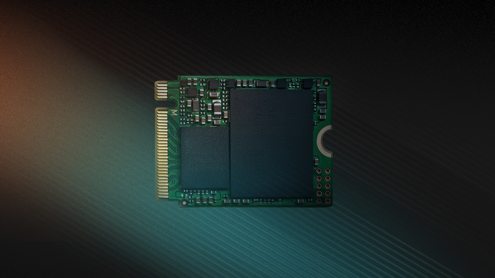
SK hynix has unveiled H-TPU, an architecture of small specialized processors designed to cut the power and area used by the internal tasks of solid-state drive (SSD) controllers. The approach splits the workload across roughly 100 lightweight processing units, instead of leaving all operations to general-purpose CPU cores, which are typically Arm-based. According to the company, each H-TPU uses around 40 times less power and takes up 25 times less area than a conventional reference core.
SK hynix’s H-TPU in 20 seconds
- H-TPU stands for Hynix Transaction Processing Unit and is designed to run repetitive tasks inside SSD controllers.
- The architecture uses around 100 small specialized processors that activate depending on the workload.
- SK hynix says each unit consumes 2.5% of the power and takes up 4% of the area of a reference CPU core.
- Arm cores still handle complex tasks, such as error recovery and exception handling.
- The company plans to bring H-TPU to enterprise SSDs and future storage solutions, including its Storage Next architecture.
The approach was unveiled at the ISOCC 2026 conference, held in Songdo, South Korea. There, SK hynix vice president Gu In-je explained that the general-purpose processors used in controllers are hitting power and area limits as SSD speeds keep increasing.
The idea isn’t to remove the CPU from the controller, but to avoid having it handle every operation. In modern drives, a large share of the work consists of processing read and write requests, managing metadata, and controlling buffers. These are tasks that repeat constantly and, according to SK hynix, can run on much simpler processors.
H-TPU: Small Processors to Spread the Work Inside the SSD
A controller is the component that coordinates how an SSD works. It manages communication with the system, organizes access to NAND memory, and handles the internal operations needed to keep the storage running.
Traditionally, much of that work falls to CPU cores built into the controller itself. These processors can run varied instructions and handle complex situations, but that versatility comes at a cost in power draw and silicon area. As the volume of operations grows, adding more general-purpose processing can become inefficient when many of the tasks are simple and repetitive.
H-TPU aims to change that balance. The name stands for Hynix Transaction Processing Unit, a lightweight, programmable processing unit SK hynix developed to run specific functions along the data input/output path.
Its responsibilities include handling read and write commands, managing metadata, and controlling buffers. Instead of processing all of these operations through the general cores, the controller can spread them across roughly a hundred H-TPUs.
The company describes an architecture in which each specialized processor handles a given function. When a request comes in, only the units needed to handle it are activated, while the rest can stay idle. This lets the workload adapt to the type of operation and avoids keeping all processing resources active all the time.
The Arm cores, meanwhile, keep handling tasks that need more flexibility, such as error recovery, exception handling, and storage policy management. The architecture combines general-purpose processing with specialized units, rather than fully replacing one type of processor with another.
A Simpler Design to Cut Power and Area
The technical difference lies in how these processors are built. According to the information SK hynix presented, H-TPU uses a four-stage pipeline with in-order execution. In simple terms, it uses a stripped-down structure that processes instructions in sequence, without most of the complexity found in CPUs designed for general-purpose workloads.
The company says each H-TPU consumes about 2.5% of the power of a reference CPU core and takes up around 4% of its area. Put another way, the conventional core used for comparison would consume roughly 40 times more power and take up about 25 times more space than a single H-TPU unit, according to those figures.
These numbers need to be read carefully. The comparison is about individual processors, not the total power draw of a whole controller or a finished SSD. The architecture packs in many specialized units, so the overall savings will depend on how many are active, what tasks they run, and the product’s configuration.
SK hynix also hasn’t quantified, in the information published, how much this will raise IOPS — input/output operations per second — or what concrete improvement it will bring to a commercial drive’s read and write speeds. So the per-processor power reduction can’t yet be translated into a specific wattage saving or a defined performance figure for end users.
The company has said it has developed programming tools to make its engineers’ work easier, including a dedicated compiler for writing code for the H-TPUs. That’s an important piece, since an architecture with so many specialized units needs tools that can assign tasks and support firmware development.
From Enterprise SSDs to Future HBF Memory
SK hynix plans to bring H-TPU to enterprise SSD controllers and extend the technology across several NAND memory product families. It also plans to use it in Storage Next, a storage architecture designed to address the data-access needs of AI systems.
According to the presentation covered by Korean outlet The Elec, Storage Next aims to work with data units of 512 bytes or smaller, compared with the 4-kilobyte blocks used in traditional access schemes. That’s a unit eight times smaller than a 4 KB block, pointing to a design built for smaller requests.
The company is also looking at bringing H-TPU to high-bandwidth flash (HBF) memory, which it expects to launch in 2027 according to the published information. That timeline is the company’s own forecast, not confirmation that every H-TPU product will reach the market by that date.
Storage for AI is placing growing demands on controllers, which have to coordinate a rising volume of requests while keeping power draw in check. In that scenario, splitting tasks across specialized processors could be an alternative to simply adding more general-purpose cores.
It’s still unclear what results H-TPU will deliver in commercial products and how it will compare with other architectures. The announced figures describe a significant cut in power and area per processing unit, but on their own they don’t predict the overall improvement for an SSD. What’s interesting about the approach is that it changes how work is organized inside the controller, just as memory and interface speeds are pushing controllers to handle more operations.
Frequently Asked Questions
What is SK hynix’s H-TPU?
H-TPU stands for Hynix Transaction Processing Unit. It’s an architecture of small, programmable processors designed to handle repetitive tasks inside SSD controllers.
How much power does an H-TPU use compared with a conventional CPU core?
SK hynix says it uses about 2.5% of the power of a reference CPU core and takes up 4% of its area. These figures compare individual processors, not complete SSD units.
Will H-TPU make SSDs faster?
The goal is to manage the controller’s internal operations more efficiently. SK hynix hasn’t published, in the cited information, a specific improvement in IOPS or read/write speeds for a commercial SSD.
When will H-TPU reach SK hynix’s products?
The company plans to apply it to enterprise SSDs and other NAND product families, as well as Storage Next and future HBF memory. The published information points to 2027 for HBF, but gives no firm dates for the full lineup.
