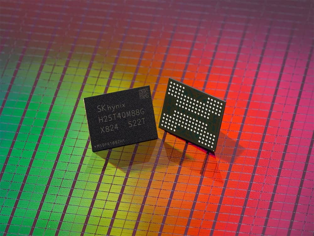
The race for memory density has just reached a new peak. SK hynix, one of the world’s leading semiconductor manufacturers, announced the start of mass production of the first 321-layer 4D NAND QLC memory, setting a historic industry record and directly targeting data centers for artificial intelligence, where energy efficiency and maximum capacity are vital.
The device, with 2 terabits (Tb) per chip, doubles the capacity of previous solutions and will spearhead a new generation of ultra-high-capacity SSDs, initially for PCs and later for enterprise sectors (eSSD) and smartphones with UFS technology.
More bits per cell: from SLC to QLC and beyond
NAND memory is classified based on how many bits each cell can store:
- SLC (1 bit): maximum speed and reliability, but costly and low density.
- MLC (2 bits) and TLC (3 bits): standard in most current SSDs.
- QLC (4 bits): higher density and lower cost, at the expense of reduced endurance.
- PLC (5 bits): still experimental, with significant reliability challenges.
SK hynix’s commitment to 321-layer QLC combines record density with mitigation techniques to minimize the traditional disadvantages of this technology.
The speed challenge and their solution
One major issue with high-capacity QLC NAND is performance loss during simultaneous operations. To address this, SK hynix increased the number of “planes” from 4 to 6, meaning independent operation units within the chip.
This architectural change has had a direct impact:
- Transfer speeds doubled compared to previous generations.
- Write performance increased by 56%.
- Read performance increased by 18%.
- Energy efficiency during writing improved by 23%.
These figures are significant. In AI environments, where servers process massive amounts of data with minimal energy consumption, each percentage point of efficiency translates into millions of dollars in annual energy savings.
From laptops to AI data centers
SK hynix’s roadmap is clear:
- First: integration into PC SSDs, where consumers demand higher capacity at competitive prices.
- Second: move into enterprise SSD (eSSD) for data centers.
- Third: reach premium smartphones with UFS, in a market demanding more space for generative AI applications on mobile devices.
The ultimate goal is to penetrate the AI server market, where SK hynix aims to differentiate itself with its 32 Die Package (32DP) technology, capable of stacking up to 32 chips in a single package—multiplying density without increasing physical size.
The context: memory as a bottleneck in AI
The AI boom has tested global storage infrastructure. Multimodal generative models trained with trillions of tokens generate unprecedented volumes of data—from training datasets to temporary inference storage.
- According to IDC, AI data lakes account for over 25% of annual enterprise storage growth.
- SemiAnalysis estimates that ultra-capacity AI SSDs will reach a $25 billion market by 2027, driven by large-scale GPU architectures.
In this scenario, SK hynix’s combination of high-density QLC and energy efficiency could become a crucial competitive advantage over rivals like Micron, Samsung, or Kioxia.
A strategic move toward “full-stack AI memory”
The company has made it clear: its goal is to become an all-in-one provider of memory for AI, combining high-performance DRAM (HBM3E), ultra-capacity NAND, and advanced 3D packaging.
“By beginning mass production, we’ve greatly expanded our portfolio and secured cost competitiveness,” stated Jeong Woopyo, head of NAND development at SK hynix. “We will make a major leap as a full-stack AI memory provider, aligning with the explosive growth in data center demand.”
They emphasize that the key isn’t just density—it’s the ability to deliver energy-efficient solutions in a context where AI data centers could consume up to 12% of U.S. electricity by 2028, according to the U.S. Department of Energy.
The horizon: toward 500 layers?
The inevitable question is: how far can layer stacking go? Today, with 321 layers in QLC, SK hynix has set an unprecedented bar. But analysts suggest that breaching the 500-layer psychological barrier could happen before 2030, with PLC (5 bits per cell) and new 3D packaging techniques.
However, each leap adds complexity in:
- Reliability: increased risk of wear and errors.
- Latency: more layers mean longer access times.
- Manufacturing costs: wafers and stacking processes are becoming increasingly expensive.
Conclusion
With its 321-layer, 2Tb QLC NAND, SK hynix not only sets a technical record but also points the way for storage in the AI era. In a market where memory is as critical as computing power, this innovation is poised to be a key piece enabling data centers to scale without collapse in energy consumption or costs.
The challenge will not only be technological but also economic and environmental: how to deliver more capacity at lower costs and with less energy impact. SK hynix appears determined to lead in this race.
Frequently Asked Questions (FAQ)
What does QLC mean in NAND memory?
QLC stands for Quad-Level Cell, a technology that stores 4 bits per cell, allowing higher density and lower cost compared to SLC, MLC, or TLC, but with reduced endurance.Why is reaching 321 layers significant?
It’s the first time NAND has exceeded 300 layers with QLC, enabling double the capacity and improved performance over older generations, especially in speed and power efficiency.Where will this memory be used first?
Initially in PC SSDs, then in enterprise SSDs for AI data centers, and high-end UFS smartphones.What impact does it have on AI?
AI models require massive data storage and processing. This high-density QLC memory will facilitate creating more efficient, ultra-capacity SSDs, promoting expansion of AI factories.
via: SK hynix news