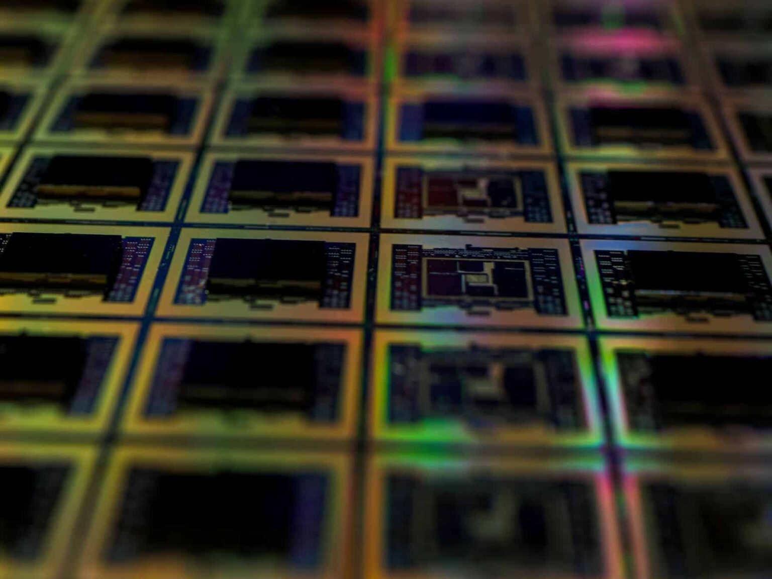
SEMIFIVE and ICY Tech have announced the tape-out of a new Edge AI SoC based on 8 nm eMRAM memory, developed using Samsung Foundry’s 8LPU technology. This milestone brings Asia closer to the first commercialization of this technology in AI chips for low-power devices—a field that is gaining importance with AI PCs, private agents, robotics, and intelligent systems that need to operate without always relying on the cloud.
The announcement is significant because it addresses one of the key limitations of Edge AI: how to run increasingly capable models on devices with constraints on energy, space, and connectivity. SEMIFIVE and ICY Tech claim that their architecture can support inference directly on the device for models of up to 2 billion parameters. At that scale, practical tasks such as text summarization, translation, or basic conversation can be performed without a constant internet connection.
eMRAM: a Non-Volatile Memory for More Efficient AI Chips
Memory is one of the most delicate components in AI chips. Fast computing units alone are not enough; data movement must also be efficient. In edge devices, where power consumption and chip area are critical, the choice of memory can make a significant difference.
eMRAM, or embedded Magnetic Random Access Memory, is an integrated variant of MRAM inside a SoC. Unlike DRAM, it does not require periodic refresh operations to retain data. Compared to flash memory, it offers faster access for certain embedded uses. And relative to SRAM, it can achieve higher density in the same space by using smaller bit cells, as the companies explain.
The most important trait is its non-volatility: it retains data even when power is off. This makes it attractive for devices that need quick wake-up times, low idle power consumption, or to maintain critical information without continuous energy use. In Edge AI, where many loads are executed near the user or machine, this characteristic can help reduce power consumption and improve response times.
Samsung Foundry has been developing eMRAM as a special embedded non-volatile memory technology for years. Their public documentation presents it as a solution compatible with CMOS logic, offering advantages in speed, high-temperature reliability, density, and energy savings. Samsung’s roadmap includes expanding eMRAM to more advanced FinFET processes, including 8 nm.
A SoC Designed for Offline AI Inference
The project combines ICY Tech’s Processing Near Memory (PNM) technology with SEMIFIVE’s SoC design platform. The idea is to bring computation closer to the memory, reducing data movement and increasing inference efficiency. ICY Tech contributes its expertise in magnetism, spintronics, and MRAM circuit design, including high-bandwidth read acceleration and in-situ matrix-vector multiplication architectures.
SEMIFIVE, in turn, has fabricated this architecture into silicon ready for production. The South Korean company is a Design Solution Partner within Samsung Foundry’s SAFE ecosystem and works on custom ASIC projects for AI, HPC, and edge AI. This is their first ASIC design project based on eMRAM, broadening their portfolio toward architectures that combine advanced memory with AI acceleration.
The commercial goal is clear: devices capable of executing AI models locally, with low latency, and without constantly transmitting data to external servers. This applies to AI PCs, private assistants, humanoid robots, automotive electronics, digital cabins, autonomous driving systems, and smart devices. In all these cases, privacy, quick response, and offline availability can be as important as raw power.
| Element | Contribution to the project |
|---|---|
| Samsung Foundry 8LPU | 8 nm process used to manufacture the SoC |
| eMRAM | Integrated non-volatile memory with lower standby power |
| ICY Tech | PNM architecture, custom MRAM, and inference acceleration |
| SEMIFIVE | Complete ASIC design and silicon-ready fabrication |
| Edge AI | Local execution of models without always relying on the cloud |
| Up to 2B parameters | Range announced for tasks like summarization, translation, and conversation |
Why It Matters for Robots, AI PCs, and Automotive Applications
Edge AI is no longer just a secondary category. For years, much of advanced AI depended on data centers. While that architecture remains essential for training large models and supporting complex applications, it is not always sufficient. There are use cases where sending data to the cloud introduces latency, power consumption, costs, network dependence, or privacy risks.
For example, a humanoid robot cannot always wait for a response to travel to a remote server and back. A vehicle needs to make decisions with low latency. A personal AI-enabled computer can offer more privacy if some tasks are executed locally. An enterprise private agent may need to process sensitive data without exposing it to external services.
Technologies like eMRAM and PNM are relevant here. Reducing data movement within the chip is one of the most direct ways to save energy. In AI, many operations are not limited solely by computation but also by the constant transfer of weights and activations. If part of this work occurs close to the memory, efficiency can be improved.
Manufacturers present this SoC as a way to overcome some limitations of SRAM-based edge designs, where area and power constraints make it difficult to host larger models on the device. It’s prudent to wait for independent performance, power, cost, and production data before drawing firm conclusions. While tape-out marks a significant design milestone, it does not yet mean commercial mass production or market validation.
This chip also reflects a broader trend: AI semiconductors are becoming more specialized. Not everything will be a data-center GPU. We will see ASICs for local inference, NPUs for PCs, automotive accelerators, chips for robots, advanced memory, and architectures tailored to specific workloads. As AI moves closer to the device, custom-designed solutions will gain importance over generic ones.
A Sign of Asia’s Edge AI Race
The announcement also has an industrial interpretation: Asia aims to secure a strong position not only in advanced manufacturing but also in custom chips for edge AI. SEMIFIVE, ICY Tech, and Samsung Foundry combine ASIC design, emerging memory, and fabrication processes into a product aimed at commercial applications. If it proceeds toward mass production, it could reinforce Samsung Foundry’s role in advanced eMRAM technologies and provide SEMIFIVE with a notable case in non-conventional memory ASICs.
For ICY Tech, the tape-out confirms the transition from magnetism and spintronics research to real silicon. The company, spun out from Beijing University’s Applied Magnetism Center, seeks to differentiate with high-bandwidth MRAM architectures for inference. In a market filled with NPUs, compact GPUs, and proprietary accelerators, this differentiation could be valuable if they demonstrate performance per watt and cost-effectiveness.
The next step will be to verify if the chip meets the promised performance outside the announcement. Samples, real-model testing, customer validation, manufacturing costs, thermal performance, and a clear volume road map will be necessary. In semiconductors, tape-out concludes the physical design and sends the chip to fabrication, but the commercial story begins afterward.
The direction is certainly meaningful: local AI needs more than small models. It requires chips capable of efficient inference, integrated memory to reduce power, and architectures designed for specific tasks. The 8 nm eMRAM technology could become a key candidate for this new generation of intelligent devices.
Frequently Asked Questions
What have SEMIFIVE and ICY Tech announced?
They announced the tape-out of an edge AI SoC based on 8 nm eMRAM, developed via Samsung Foundry’s 8LPU process, aimed at low-power local inference.
What is eMRAM?
It is integrated magnetic memory that retains data without power, does not need periodic refreshes like DRAM, and can help reduce power consumption in embedded devices.
What does support for models of up to 2 billion parameters mean?
It indicates that, according to the companies, the architecture can run AI models of up to 2 billion parameters directly on the device—for tasks like summarization, translation, or basic conversation.
In which devices could this technology be used?
Applications include AI PCs, private agents, humanoid robots, automotive systems, digital cabins, autonomous vehicles, and smart devices requiring local inference.
via: prnewswire