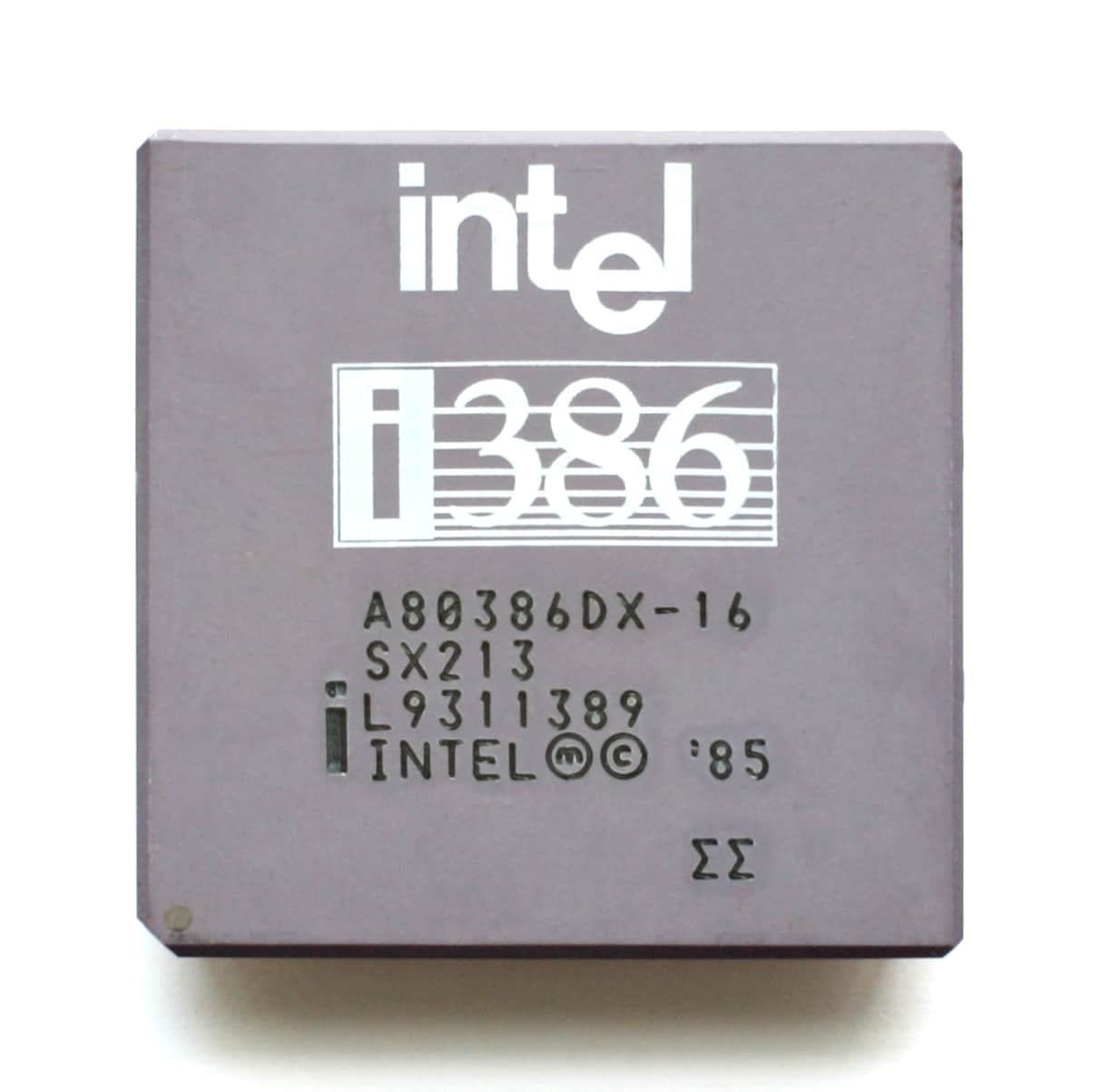
In an era of processors with thousands of contacts and ultracompact packages, the Intel 386 may seem like a relic: a gray ceramic block with 132 gold pins, common on motherboards from the late 1980s and early 1990s. However, behind that plain exterior lies an engineering marvel that marked a turning point in microprocessor history.
Thanks to a computed tomography (CT) scan carried out by Ken Shirriff, it has become possible to observe, layer by layer and without physically touching the chip, the complex internal structure that enabled the leap to modern multitasking computing. What looks like a simple ceramic package turns out to be a highly sophisticated multilayer system, comparable to a miniature motherboard.
A journey to the heart of an icon
The Intel 386, launched in 1985, was the first 32-bit x86 microprocessor capable of true multitasking and addressing large amounts of memory for its time. It became the foundation for a generation of personal computers and workstations that laid the groundwork for the modern PC.
Externally, the processor appears as a 132-pin ceramic pin grid array (PGA) designed to fit into a socket for easy replacement. But the real interest lies inside: a custom encapsulation design that broke the limitations of Intel’s early processors, which until the mid-1970s rarely exceeded 16 pins due to a more cost-focused approach than technical necessity.
CT scans as a lens of the 21st century
Shirriff, in collaboration with Lumafield, used an industrial CT scanner to scan the chip. The result: hundreds of microscopic slices combined digitally to generate an interactive 3D model. This allows virtually “peeling” each layer of the package and analyzing the arrangement of pins, wires, and power planes.
The first surprise when digitally removing the outer layer is the halo of ultra-fine gold wires—about 35 micrometers thick, thinner than a human hair—that connect the tiny silicon die to the internal leads of the package. Some wires carry data or control signals, while others group up to five connections to handle the high current demands of power and ground lines.
A package that’s essentially a six-layer circuit board
Scanning reveals that the 386’s package functions like a miniature multilayer printed circuit board. It consists of:
- Two internal signal layers, transporting data and control signals.
- Four dedicated copper planes for power and ground, providing clean, stable energy to different parts of the chip.
This layout minimizes interference and voltage drops, critical for a high-performance processor of its era. The connection method, called “single-row double-shelf bonding,” employs two concentric levels of pads around the die to maximize interconnection density.
Thermal and mechanical engineering
Underneath the silicon die, the scan uncovers a bright zone filled with silver-loaded epoxy. This material isn’t just an adhesive; it serves a dual purpose—conducting heat away from the die to the package for dissipation, and providing a low-resistance electrical ground connection to enhance stability.
This combination of thermal management and electrical robustness was essential for the 386 to operate reliably under load, contributing to its longevity and dependability.
Scaling from micrometers to millimeters
The package acts as a scale translator. Within the die, structures measure roughly 1 micrometer; internal traces grow to 6 μm; the die pads are separated by 0.25 mm; the pads on the package are 0.5 mm apart; and the pins inserted into the motherboard are 2.54 mm. Overall, there is approximately a 2,500-fold size increase from the internal logic to the visible connections.
The mysterious “NC” pins and production secrets
Another significant find involves eight “NC” (No Connect) pins, officially unused for connection to the motherboard. However, analysis indicates that seven of these pins almost have the entire internal infrastructure prepared—they have pads on the die, traces on the package, and even holes for bond wires, missing only the wire itself. This suggests they might have been reserved for special versions or internal diagnostics during manufacturing.
Even more interesting, one of these NC pins is actually connected and seems to function as an output, possibly for internal signals that Intel chose not to publicly document.
Hidden side contacts
The CT scan also revealed the presence of micro side contacts inside the package, used during manufacturing to gold-plate the pins. These contacts are nearly invisible to the naked eye but detectable with a multimeter and are typical in ceramic packages from that era—though little known outside the industry.
Two separate power and ground networks
One of the most intriguing technical discoveries is that the 386 has two independent power and ground networks: one for the internal logic and another for I/O controllers. This separation minimizes interference caused by rapid switching in data lines, helping stabilize the core logic.
On the motherboard, these networks are connected, but decoupling capacitors absorb current spikes on the I/O lines to prevent disturbance to the rest of the chip.
Manufacturing the ceramic package
The multilayer package is produced from “green sheets”—ceramic-based flexible foils with powder and binder. After perforating these sheets to form vias, tungsten paste is printed to create traces. The layers are stacked, laminated under pressure, and sintered at 1,500–1,600 ºC.
Pins are then soldered, gold-plated with internal contacts, the die mounted, gold bond wires attached, and finally, sealed with a metal lid. The entire assembly is tested, labeled, and shipped.
A strategic shift at Intel
The 386 also symbolizes a strategic change at Intel. Early on, the company aimed to limit pin count to reduce costs—impacting early chips like the 4004 or 8008. With the 386, Intel abandoned that philosophy, adopting high-density packages essential for handling 32-bit buses and multiple power lines.
The cost of this package was so high that, over time, it equaled the die’s price itself. To cut costs, Intel introduced cheaper plastic versions (PQFP).
From past to present: the scale of progress
Comparing the 386 to modern processors is eye-opening. While this classic had 132 pins, a current Xeon can feature over 7,500 contacts, and a typical laptop CPU surpasses 2,000 in BGA format. Power, thermal, and signal integrity needs have grown exponentially, but the fundamental concept of encapsulation as a physical-silicon interface remains.
Conclusion: the value of looking inside
Ken Shirriff and Lumafield’s work not only satisfies retro hardware enthusiasts but also reminds us that packaging engineering is as crucial as the processor’s logical design. For the Intel 386, it was the combination of both that enabled the leap to multitasking and 32-bit architectures that dominated for decades.
Using modern tools like CT scans to examine this processor is, in a way, opening a time capsule—appreciating how, within a small space and with 1980s technology, problems still relevant today were addressed.
FAQ
1. Why was the Intel 386’s package so advanced for its time?
Because it integrated a multilayer design with dedicated power planes, ultra-fine gold wires, and materials like silver-loaded epoxy to ensure stability, low interference, and efficient heat dissipation.
2. What is the function of the “NC” pins on a processor?
Although officially unused, they can serve as reserves for debugging, internal testing, or custom versions of the chip.
3. How was the ceramic package manufactured?
Using “green sheets” with printed tungsten traces, stacked, laminated, sintered at high temperatures, with pins soldered, gold-plated, and connected via wire bonding.
4. Why is separating power networks within a chip important?
It isolates the core logic from the fluctuations caused by rapid I/O switching, reducing errors and boosting reliability.