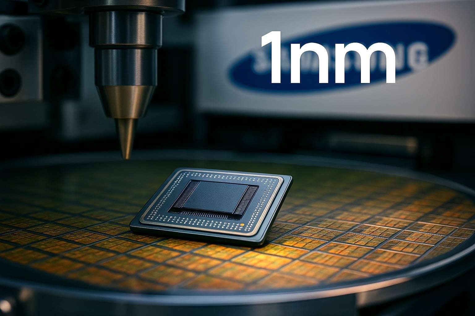
Samsung Foundry is once again looking toward the most extreme future of miniaturization with a new long-term goal: to bring its manufacturing process to 1 nanometer by 2031. The information comes from the South Korean financial newspaper Korea Economic Daily, which claims that Samsung’s foundry division aims to complete R&D on this node by 2030 and then move it into production, relying on an architecture known as forksheet to increase transistor density on the same chip surface. However, for now, this is not an official Samsung announcement but a roadmap published by local press and based on industry sources.
This news aligns with a broader sector trend: as classical scaling becomes more difficult and expensive, manufacturers need architectural changes, not just nominal node reductions. In this context, Samsung’s idea makes technical sense. The Korean media explains that the forksheet would introduce a non-conductive wall between GAA (Gate-All-Around) devices to bring them closer and thus increase the number of transistors in the same space. Put simply, it would be an evolution of current GAA to extract more density when further physical shrinking is no longer sufficient.
What’s confirmed and what remains an unofficial road map
Here, it’s important to distinguish between confirmed facts and industry speculation. Samsung has publicly confirmed its strategy for 2 nm. In technical documentation and previous presentations, the company has detailed the SF2 family, with variants like SF2P for 2026 and SF2A for automotive applications in 2027. Additionally, Samsung announced in 2024 specific collaborations on 2 nm GAA technology, such as the agreement with Preferred Networks to produce AI accelerators on this node and integrate 2.5D packaging.

What remains unconfirmed officially is the leap to 1 nm in 2031 with the forksheet architecture. Samsung has not yet published a corporate note validating this specific timeline. Therefore, any interpretation should treat it as a reported industry plan, not a firm promise. Especially since Samsung’s recent history with advanced nodes has been marked by schedule adjustments, competitive pressures from TSMC, and recurring doubts about performance and yields.
Why the forksheet matters so much
The technical crux of the rumor lies in the forksheet. This architecture is considered an evolution of nanosheet transistors within the GAA paradigm. Instead of merely stacking and wrapping the channel, the forksheet aims to further reduce the separation between devices by inserting a dielectric wall that allows more functional structure within the same area. It’s not just an incremental improvement: it’s the kind of architectural leap the industry needs when Moore’s Law can no longer be sustained solely through finer lithography.
Samsung would not be the only company exploring this path. In the semiconductor ecosystem, the forksheet has long been discussed as a possible intermediate phase between GAA and even more complex architectures like CFET. While the Korea Economic Daily report is not yet officially confirmed by Samsung, the technological basis of the idea aligns coherently with current research trends in sub-2 nm nodes.
The main challenge for Samsung is not 1 nm: it’s 2 nm
Samsung’s ambitions sound promising on paper, but the market knows the real test comes much earlier. Before talking about 1 nm, Samsung needs to convince clients and analysts that its 2 nm GAA is competitive in performance, power consumption, performance per watt, and manufacturing capacity.
This is the critical point. The company has been working to strengthen its foundry business and narrow the gap with TSMC, but still lags significantly in market share. According to TrendForce, TSMC remained the global leader in foundry sales in 2025 with a commanding advantage, while Samsung held second place but at a considerable distance.
In other words, the discussion about 1 nm helps project technological prowess and aspiration to potential customers, but the real priority for Samsung is elsewhere: proving that its 2 nm roadmap results in chips that meet targets for efficiency, yields, and schedule.
The race is also commercial, not just technical
This Korean approach links the effort to attract major tech clients. That also makes sense. In foundry, success is not only about smaller nodes but about volume contracts, operational confidence, and execution capacity. Samsung is trying to reinforce its long-term narrative, especially as the AI market fuels demand for advanced chips and each new node becomes a commercial tool for winning multimillion-dollar orders.
This is the strategic takeaway: even if 1 nm appears distant, announcing or hinting at a roadmap toward it signals to the market that Samsung remains in the technological race and refuses to accept being a perpetual runner-up behind TSMC. However, in semiconductors, credibility is built not on promises for 2031, but on what each factory and each node deliver in the next two or three years.
What could happen now
The most reasonable expectation is for more official signals at upcoming Samsung Foundry events or future roadmap updates. If the 1 nm plan with forksheet is real and not just exploratory, it should start to appear in more concrete presentations, customer documents, or technical forums over the coming years.
Until then, this news should be read as what it truly is: a sign of serious technological ambition, but not yet a confirmed industrial reality. Samsung wants to be in the 1 nm conversation, yes. But the market will first require something more immediate and much more challenging: for its 2 nm to cease being only an aspiration and become a credible alternative to the sector’s leader.
Frequently Asked Questions
Has Samsung officially announced its 1 nm process for 2031?
Not officially at this time. The information comes from Korea Economic Daily, citing an internal plan or a roadmap reported by industry sources.
What is forksheet technology?
It’s an evolution of GAA/nanosheet architecture that adds a dielectric wall between devices to reduce separation and pack more transistors into the same area.
What has Samsung officially confirmed about advanced nodes?
Samsung has publicly announced its SF2 family on 2 nm, including variants like SF2P, and partnerships for manufacturing AI chips on 2 nm GAA.
What is Samsung’s biggest current challenge?
More than 1 nm, the immediate challenge is to make its 2 nm process competitive in performance, efficiency, and manufacturing capability against TSMC.