Samsung Electronics has decided to revive its Z-NAND memory technology, abandoned seven years ago, in order to meet the growing demand for performance in artificial intelligence (AI) workloads. The South Korean company positions this solution as a high-speed alternative to traditional NAND, promising up to 15 times faster access and processing speeds for critical applications.
This announcement comes at a time when the memory market faces increasing pressure from generative AI, high-performance data centers, and edge computing applications. Industry sources indicate that Z-NAND aims to serve as a bridge between DRAM—fast but volatile—and conventional NAND flash—more affordable but with higher latencies—offering a balance of cost and performance for scenarios requiring ultra-low response times.
A technology making a grand comeback
Introduced in 2016, Z-NAND was developed as a response to Intel and Micron’s emerging 3D XPoint memory. However, due to limited adoption and advancements in TLC and QLC NAND, Samsung decided not to proceed with large-scale commercialization at that time.
Now, with the explosion of AI and the need to process massive volumes of data in real time, the company is resuming the project with an architecture optimized for tasks such as AI model training and inference, financial data analysis, medical image processing, and scientific simulations.
Direct competition in the AI memory ecosystem
The revival of Z-NAND also addresses the rising competition in high-performance memory sectors. Companies like Kioxia, Micron, and SK hynix are investing in technologies like XL-FLASH and HBM (High Bandwidth Memory) to meet AI accelerator demands. Samsung aims to differentiate itself with a product that, according to analysts, could be more affordable than HBM and faster than conventional NAND, providing greater durability and energy efficiency.
Key applications and market outlooks
The new generation of Z-NAND targets several applications, including:
- Generative AI data centers: training and inference of large models with minimal latency.
- Industrial edge computing: real-time data analysis and responses in critical environments.
- Financial systems and algorithmic trading: executing operations in real time.
- Scientific and medical processing: high-resolution simulations and image analysis.
Analysts estimate that if Samsung can produce Z-NAND at a competitive scale, it could capture a sizable share of the AI memory market, projected to reach billions of dollars by the end of the decade.
Frequently Asked Questions (FAQs)
What is Z-NAND memory?
It is a non-volatile flash memory technology developed by Samsung that offers significantly faster access speeds than traditional NAND, with lower latency and higher endurance, designed for high-performance applications.
Why did Samsung stop producing Z-NAND in the past?
Its initial adoption was limited, and the market favored more economical solutions like TLC and QLC NAND, while DRAM remained the preferred choice for low latency.
How does Z-NAND differ from HBM?
HBM (High Bandwidth Memory) provides much higher bandwidth and is integrated directly into accelerators like GPUs, but it is more expensive. Z-NAND, although slower than HBM, is more cost-effective and can be used in high-speed storage systems.
What are the most promising applications for Z-NAND?
AI workloads, financial data processing, scientific analysis, medical imaging, and industrial edge computing.
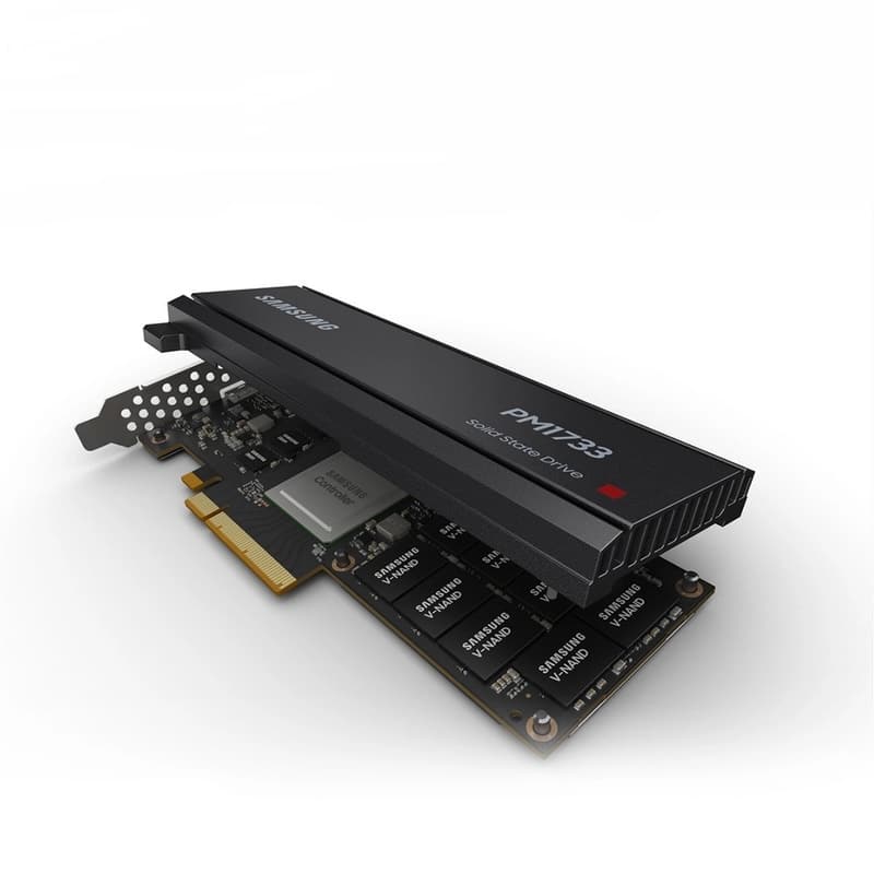
Photo via: storagesserver.com