Samsung Electronics is accelerating the modernization of one of the least visible but most sensitive steps in semiconductor manufacturing: dicing or wafer cutting. According to South Korean daily ETNews published on March 24, the company is ordering new femtosecond laser cutting equipment to expand its use in producing HBM4, the high-bandwidth memory set to drive the next generation of AI systems. While Samsung has not issued a specific statement regarding these orders, the information aligns with the company’s roadmap since the beginning of the year to strengthen its position in advanced memories.
This news matters because wafer cutting is not a secondary phase. After circuits are patterned on the wafer, each chip must be separated with maximum precision. In increasingly dense, stacked, and AI-oriented memories, any improvements in cleanliness, thermal damage, or die integrity can impact final performance, reliability, and especially fab yield measured in usable wafers. Therefore, Samsung’s move to adopt more advanced cutting technology as HBM4 enters commercial production appears to be a strategic industry move rather than a minor adjustment.
A technical shift with direct impact on yield and productivity
According to ETNews, Samsung is preparing orders for at least 10 femtosecond laser dicing systems for both grooving—creating the initial groove on the wafer—and full cut, with plans to install them at its Cheonan campus, one of its facilities dedicated to semiconductor assembly, testing, and packaging. The same source mentions that the company is considering increasing the volume of these purchases, partly because delivery times for such machinery exceed eight months. This should be read as supply chain and industry source information, not as an official detailed confirmation from Samsung.
There is solid technical backing for this change. DISCO, a leading global specialist in wafer dicing and processing equipment, explains in its technical documentation that short and ultrashort pulse laser systems allow for reduced thermal damage and improved cut quality compared to conventional approaches. Their analyses conclude that ultrashort pulse lasers followed by blade dicing decrease fusion at the groove base and enhance die resistance to stress, compared to traditional laser and mechanical cuts. In essence, it’s not just about finer cuts, but doing so with less stress on the chip.
With femtosecond lasers, the accuracy boosts another level. Unlike nanosecond pulses, ultrashort pulses operate at a much finer scale and limit heat-affected zones more effectively. For products like HBM4, where stacking complexity, interconnection density, and advanced packaging demands are increasing, such improvements can be particularly significant. The information published in Korea indicates that Samsung aims to prioritize this technology in HBM4 to elevate both quality and productivity.
HBM4 is no longer a promise but an ongoing industrial race
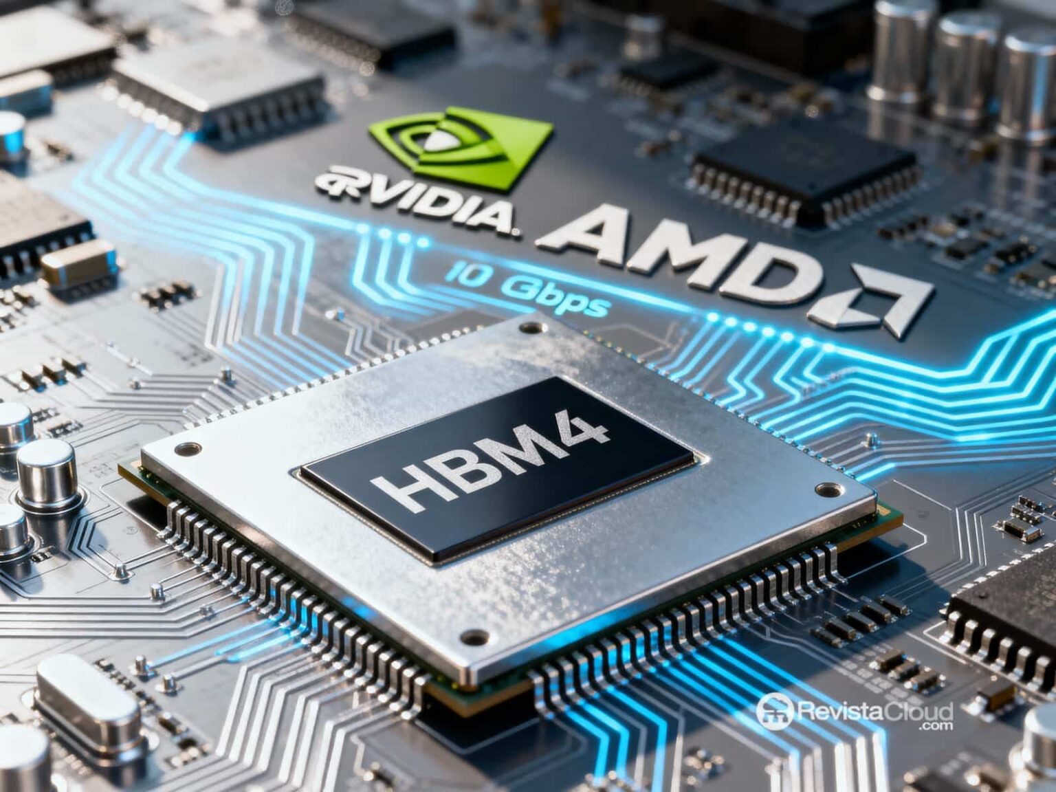
The context further clarifies this decision. Samsung announced on February 12 that mass production of HBM4 had begun and that commercial products were already being shipped to customers. The same announcement highlighted that HBM4 achieves a steady speed of 11.7 Gbps, expandable up to 13 Gbps, and that this generation targets data centers and the new wave of AI infrastructure. Shortly after, at GTC 2026, the company showcased HBM4 and HBM4E as central components of its next-generation AI system offensive.
Additionally, Samsung has begun publicly strengthening its commercial ties around this memory. On March 18, it announced an expansion of its strategic collaboration with AMD on AI memory solutions, including main supply of HBM4 for the upcoming AMD Instinct MI455X GPU. Reuters also reported that Samsung is seeking multi-year agreements with major clients to bring more stability to its chip business amid a “supercycle” driven by AI data centers. In this environment, process improvements that enable higher volume and better quality are immediately valuable.
Competitive pressure is evident. TrendForce noted this month that Samsung is regaining ground in HBM through HBM3E and HBM4, although SK Hynix still leads global production in bits. The firm projects SK Hynix will hold roughly 50% of HBM output in 2026, with Samsung increasing to around 28%. That’s a significant gap, explaining why the Korean group is working to refine both commercial validation and manufacturing efficiency. Reuters recalled last week that Samsung continues to try to close the gap with SK Hynix in high-bandwidth memory, a market where industrial execution quality is becoming just as critical as product design.
Beyond HBM4: a potential fundamental shift in manufacturing
One of the most interesting details from ETNews is that Samsung may not be limiting femtosecond laser analysis solely to DRAM. The report suggests the company is also exploring extending this approach to NAND and system semiconductors. If confirmed, this would mean not just a tactical upgrade for HBM4 but a broader transformation of final processing across various product families. Again, it’s important to note that this is industry speculation based on South Korean sector reports, not an official company plan.
It remains to be seen who will industrially capitalize on this new phase. ETNews places South Korea’s EO Technics and Japan’s DISCO as the best-positioned companies in the supply chain for these equipment types. DISCO already has a well-established catalog of laser saws and dicing solutions for advanced semiconductors, while EO Technics also markets laser grooving and dicing systems for thin wafers. If Samsung increases orders in coming months, this technological rivalry could intensify.
Ultimately, the most important takeaway is another: in the race for HBM4, announcing early production or securing major customer agreements isn’t enough. The real difference lies in manufacturing, in processes that often go unnoticed—cutting, assembly, testing, cleaning, stacking, and performance. If Samsung is betting on bringing wafer dicing into a new era with femtosecond lasers, it’s because it understands that the battle for AI memory won’t be decided solely by product marketing, but by the ability to deliver high volume, quality, and reliability at scale.
Frequently Asked Questions
What is wafer dicing in semiconductors?
It is the process of cutting a fully fabricated wafer into individual chips or dies. This step is critical because poor cuts can affect chip quality, particle contamination, and overall manufacturing performance.
What advantage does femtosecond laser have over conventional cutting?
Its main advantage is precision. Using ultrashort pulses reduces thermal damage and enables cleaner cuts, which is especially useful in advanced chips with fine structures and complex interconnections.
Is Samsung already mass-producing HBM4?
Yes. Samsung announced in February 2026 that it had begun mass production of HBM4 and was shipping commercial products to customers.
Why is HBM4 so important for AI?
Because it’s a memory designed to provide high bandwidth in high-performance systems like GPUs and AI accelerators. It is a critical component in training and inference infrastructure for advanced models.
via: Jukan