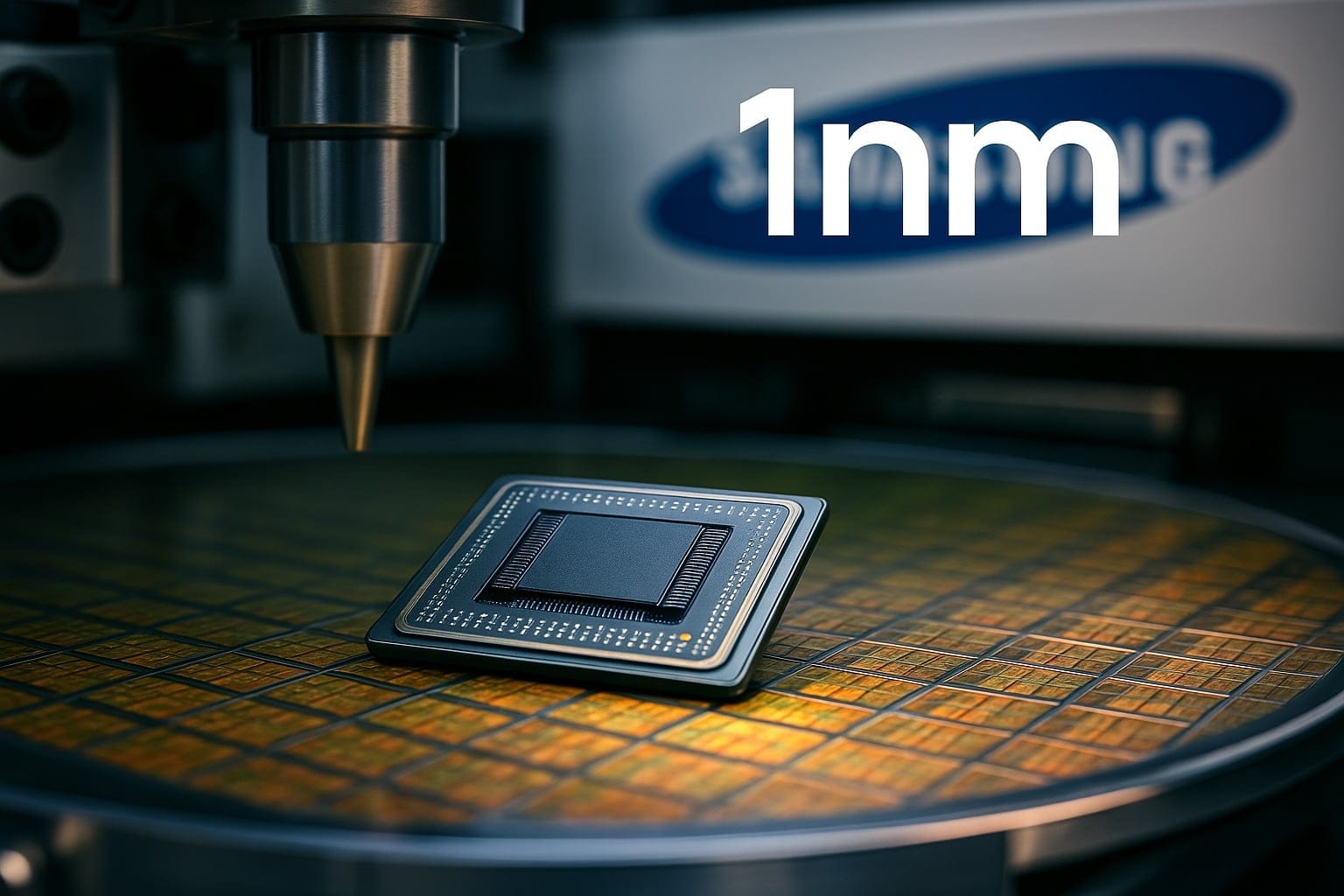
The South Korean company is improving the efficiency of its 2-nanometer process and accelerating the development of its 1 nm node, aiming to start mass production within four years.
Samsung Foundry is determined to return to the forefront of technology. After several quarters marked by challenges in performance and market share, the company has announced significant improvements in its 2 nm (SF2) processes and has officially confirmed that it is already working on the development of its 1-nanometer node, with mass production scheduled for 2029.
Advancements in 2 nm: the Exynos 2600 as a spearhead
According to the latest information, the highly anticipated Exynos 2600 will be the first system-on-chip (SoC) manufactured with the SF2 2 nm node, with mass production scheduled for November 2025. This milestone will mark a turning point for Samsung, which aims to demonstrate with this chip not only technological advances but also an operational recovery following setbacks with the 3 nm and its low initial performance levels.
The company has managed to surpass the 40% performance threshold in its 2 nm wafers, a figure still far from ideal but representing a clear improvement compared to the mere 20-30% seen at the beginning of the year. The current objective is to approach the 70-80% threshold that typically greenlights large-scale production.
“The performance of 2 nm is better than previously known. The process is more advanced than the 3 nm at this stage,” internal sources from Samsung claim.
Restructuring and commercial expansion
A significant part of this recovery is attributed to Han Jin-man, the new president of the foundry division, who has redesigned both the technical and commercial strategy. Under his leadership, Samsung has shifted its focus away from solely major U.S. clients and has actively begun diversifying into markets in China, India, and Europe. This strategy aims to secure stable revenues in mature processes and reduce the cost per wafer to improve competitiveness in advanced nodes.
Moreover, the use of GAA (Gate-All-Around) transistors in the 2 nm process will allow for improvements in performance and energy efficiency compared to the traditional FinFET, providing Samsung with a key technological advantage, especially in high-performance applications.
1 nm node for 2029: the new frontier of miniaturization
Samsung has officially begun developing its 1-nanometer process, a goal that, just a few months ago, seemed distant. The R&D team has gathered some of the engineers behind the 2 nm node to tackle this new challenge, which will involve a deep redesign of chip architecture and the use of advanced lithography tools, such as high numerical aperture (High-NA) EUV scanners.
“We are working towards starting mass production in 2029,” the company states.
With this, Samsung joins the race already underway between TSMC and Intel to conquer the sub-nanometer territory. This new generation of processes will likely require the use of Forksheet technology, an evolution of GAA transistors, and could represent the last major leap before the physical limits of miniaturization impose new rules.
TSMC remains in the lead, but Samsung sees an opportunity
Despite the advancements, Samsung is still behind TSMC in terms of production yield. The Taiwanese foundry is reported to have already reached a yield of 60% in its 2 nm process and is expected to begin mass production before the end of 2025. According to TrendForce, the gap in market share between the two has widened: TSMC closed 2024 with 67.1% compared to Samsung’s 8.1%, a drop to single digits that raised alarms in Seoul.
However, TSMC’s sustained price increases are creating opportunities for Samsung. Some sources indicate that companies like Apple and AMD are already evaluating migrating part of their production to the South Korean manufacturer’s advanced nodes, seeking a more favorable cost-performance ratio.
Conclusion: the race towards 1 nm accelerates
With its renewed strategy and ambitious timeline, Samsung aims to regain ground in the race for semiconductor supremacy. If it can stabilize the performance of its 2 nm process and maintain its momentum towards 1 nm, the company could re-establish itself as a preferred option against TSMC and Intel.
As the industry moves into the decade of sub-nanometer computing, leadership is no longer measured just by nodes but by execution capability, commercial flexibility, and cost control. And Samsung, after years of setbacks, seems determined to compete at the highest level once again.