
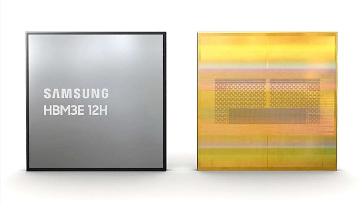
Samsung is working on a deep change to HBM memory for AI accelerators. The endpoint is zHBM, an architecture that stacks memory vertically over the processor, shortens the distance data has to travel, and drops parts of today’s 2.5D packaging. Samsung projects up to 230% more bandwidth and around 70% less DRAM power than a conventional HBM4E setup, though these are still goals it presents, not commercial product specs.
Samsung zHBM in 20 seconds
- Samsung proposes moving from conventional HBM to a three-dimensional architecture it calls zHBM.
- The memory would sit vertically over the xPU, such as a GPU or AI accelerator.
- The company estimates up to 230% more bandwidth and 70% less DRAM power.
- The development follows several intermediate stages of custom and advanced HBM.
Samsung laid this out in a technical talk about how the base die evolves: the chip at the bottom of an HBM stack. The core idea is for that component to take on functions that now live in the processor, well beyond communication, control, and testing.
It’s aimed at a problem that keeps getting more obvious in AI systems: making GPUs faster doesn’t help much if memory can’t feed them data fast enough.
Today’s HBM is starting to hit physical limits
High Bandwidth Memory (HBM) was built to solve exactly that bandwidth problem. Instead of putting conventional DRAM chips around the processor, it stacks several memory layers and connects them with vertical TSVs (Through-Silicon Vias).
An HBM stack has two main parts. The core dies, or C-die, hold the DRAM cells that store data, while the base die, or B-die, underneath handles communications along with control and testing functions.
The stack then talks to the GPU, TPU, or other accelerators through a physical, or PHY, interface.
Samsung points to that interface zone as a key roadblock to more performance. The PHY eats up meaningful space on the base die, and moving data between memory and processor costs both area and energy.
HBM’s history is mostly a story about bandwidth. Samsung cites roughly 3 TB/s per stack with HBM4, around 4 TB/s with HBM4E, and more than 6 TB/s projected for a future HBM5. Those later generations are still in development, so treat the numbers as target goals, not final specs.
But you can’t keep raising pin counts, connection numbers, or speeds forever.
AI makes it worse, because it’s no longer just about bigger models. Longer contexts and multi-user setups swell the KV cache, the temporary memory used during inference to hold token information from earlier steps.
That puts pressure on two fronts at once: capacity and bandwidth.
Samsung wants a more active, integrated HBM base
Samsung’s plan runs in three big phases.
The first trims the area that traditional physical interfaces take up.
In what it calls custom HBM (cHBM), Samsung would replace part of the conventional PHY with direct die-to-die (D2D) connections. Shorter connections should cut power and free surface area for the accelerator.
Samsung estimates this could free roughly 5-10% of the xPU’s area, with performance gains of 10-20% depending on the design. Those are its own estimates and don’t generalize to every GPU.
Packing components closer together also brings heat problems.
For that, Samsung built its Heat Path Block (HPB) technology to improve how heat escapes. By its data, it could cut the peak temperature in certain interface zones by more than 35%.
The next step is more intriguing: shifting some GPU functions straight into the HBM base die.
The memory controller is one candidate. Others could include repair mechanisms via SRAM, advanced telemetry, RAS (Reliability, Availability, and Serviceability) functions, internal testing, and controllers that can hook up extra memory modules.
That would turn memory from a fairly passive part sitting beside the processor into an active participant in how the system runs.
AHBM would bring processing closer to memory
The second phase pushes the idea further.
Samsung is looking at putting Processing Elements (PEs) inside the memory, creating what it calls Advanced HBM, or AHBM.
The reason comes back to a big cost of modern computing: moving data burns energy.
GPUs can crunch math extremely fast, but they have to keep shuttling data from memory to compute units and back, which draws a lot of power.
Cut that movement by doing operations closer to the data, and efficiency climbs.
This doesn’t mean HBM replaces GPUs. Specific functions would move into the memory only where it lowers communication and power draw.
Samsung is also weighing using the base die for expansion interfaces that connect to external memory. That’s handy for language model inference with large context windows, where the KV cache can eat tens or hundreds of gigabytes.
Which leads to the third stage.
zHBM would put memory directly on top of the processor
Today’s AI accelerators usually use 2.5D packaging.
The GPU and several HBM stacks sit close together, connected by an interposer. That gives far more bandwidth than conventional memory outside the package, but data still has to move sideways between components.
zHBM would change that geometry.
Samsung would stack the memory vertically over the xPU itself, giving a 3D architecture where processing and memory connect through very short vertical links.
That drops the traditional 2.5D interposer and lets input/output connections spread across a larger surface.
Samsung is looking at packaging techniques like Wafer-on-Wafer (WoW) and hybrid bonding to reach very high connection densities.
The company targets communication energy near 0.5 picojoules per bit.
Against a conventional HBM4E setup, Samsung’s simulations and estimates for zHBM point to 230% higher DRAM bandwidth, about 70% lower memory power, and roughly 100 watts of extra thermal headroom for the rest of the system.
Again, these are Samsung’s technological goals. zHBM still faces hurdles in manufacturing, thermals, cost, reliability, and volume production.
Memory and processor functions are starting to merge
Samsung’s approach fits a wider industry shift.
For decades, telling processor and memory apart was easy: one does the math, the other stores the information.
AI is blurring that line. Models move enormous amounts of data, and the energy spent just transporting it has become a big share of total consumption.
So memory and accelerator designers are experimenting with compute-near-memory, processing-in-memory, custom memory, and 3D packaging.
Samsung has an edge here, since it works in DRAM manufacturing, logic processes, and advanced packaging all at once.
zHBM is meant to draw on all of that.
But putting memory on top of a processor that can dissipate hundreds of watts isn’t trivial. Too much heat can hurt DRAM data retention, raise refresh needs, and complicate cooling.
Manufacturing also needs high enough yields: stacking many chips vertically means one defect can ruin a much more expensive assembly.
So Samsung isn’t proposing a jump straight from HBM4 to zHBM.
Its path goes through custom HBM first, then adds new functions to the base die with AHBM, and finally reaches the 3D integration of zHBM.
The overall direction is clear: the next leap for AI accelerators won’t come from faster GPUs alone.
It also means getting data much closer to where the processing happens.
Frequently Asked Questions
What is Samsung zHBM?
zHBM is a memory architecture Samsung proposes that vertically integrates HBM over an xPU, such as a GPU or AI accelerator. It aims to shorten communication distances, raise bandwidth, and lower power consumption.
How does HBM4 differ from zHBM?
HBM4 keeps an architecture where the processor and the memory stacks connect through advanced packaging. zHBM aims for 3D integration, with memory placed directly on top of the processor.
What performance can zHBM deliver?
Samsung projects up to 230% more DRAM bandwidth and around 70% lower power than a conventional HBM4E setup. These are estimates and development goals, not final commercial specifications.
When will Samsung zHBM be available?
No commercial release date has been announced. Samsung places zHBM as the third stage after custom HBM and Advanced HBM in its roadmap.
via: wccftech
