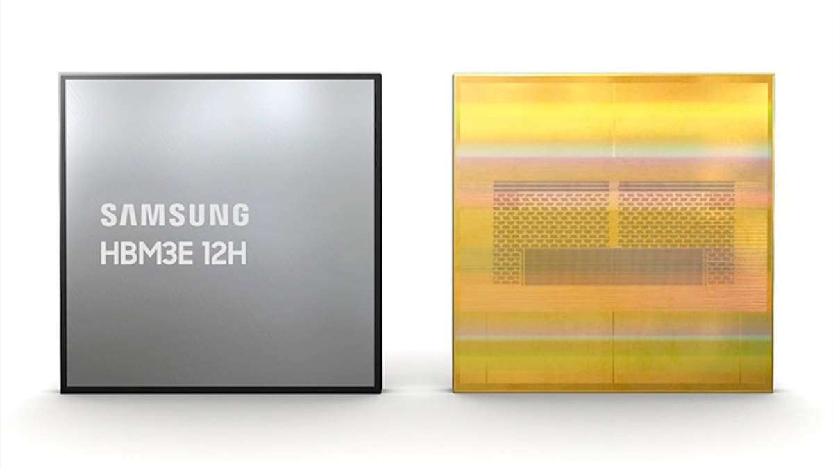
Samsung Electronics has finally passed NVIDIA’s qualification tests for their 12-layer (12-Hi) HBM3E, a milestone achieved after 18 months of effort and several failed attempts to meet the demanding performance and reliability criteria set by the global leader in AI accelerators. Confirmed by industry sources, this approval signifies a recovery of technological credibility in the most strategic high-bandwidth memory battlefield, during the ongoing race to power the next generation of AI hardware.
This achievement is more symbolic than financial at this stage: Samsung becomes the third supplier of 12-Hi HBM3E for NVIDIA —after SK hynix and Micron— leading to initial volumes that are relatively small. Still, re-entering the supply chain of the industry’s most coveted client in AI is a key move in the context industry calls the “true battleground”: HBM4.
Implications of HBM3E 12-Hi Validation
- Technical recovery: Industry sources attribute this shift to Samsung’s semiconductor boss, Jun Young-hyun, who decided earlier this year to redesign the HBM3E DRAM core to address thermal problems affecting previous versions. In 12-Hi stacks, thermal control and signal integrity are critical: more layers mean higher density, greater power density per millimeter squared, and increased risk of throttling or errors if the design isn’t robust.
- Dominant customer: While AMD was already receiving Samsung’s 12-stack HBM3E for its MI350, NVIDIA’s “green light” was still pending, being the largest consumer of advanced memory for AI workloads. The green light doesn’t guarantee large immediate orders but reopens the door to future product collaborations.
- Visitor card for HBM4: In a market where SK hynix has led HBM for NVIDIA in previous cycles, any advance that demonstrates engineering capability at the limit (12-Hi, frequencies, and reliability) improves Samsung’s negotiating position for the next-gen RAM.
What Changes with HBM3E 12-Hi Validation
- Technical comeback: Industry insiders say this move was driven by Samsung’s semiconductor head, Jun Young-hyun, who decided to redesign the HBM3E DRAM core earlier this year to fix thermal issues seen in earlier versions. In 12-Hi stacks, managing heat and signal integrity are critical: more layers lead to more density, more power per area, and increased risk if not properly engineered.
- Leading customer: Although AMD was already using Samsung’s 12-stack HBM3E for the MI350, NVIDIA’s “green light” was still awaited, as the main buyer of advanced memory for AI workloads. The approval does not mean large immediate orders but reopens the door for future product integration.
- Next-generation HBM4: In a market traditionally led by SK hynix for NVIDIA HBM, Samsung’s advancements in engineering at the limit — including engineering at 12-Hi, frequency, and reliability — enhance its position as a key supplier for this technology’s future.
The Real Focus: HBM4 and NVIDIA’s “Vera Rubin” Architecture
The industry is shifting its attention to HBM4, the sixth iteration of high-bandwidth memory, which will debut with “Vera Rubin”, NVIDIA’s successor to the Blackwell chips, starting from next year.
Samsung aims to close the gap with SK hynix by employing a mix of process technologies and architectures:
- DRAM 1c (10 nm-class) for memory dice versus 1B for some rivals.
- Logical die at 4 nm manufactured in Samsung’s foundry, compared to 12 nm used by competitors. This base die manages routing, ECC, RAS, and access via TSV (Through-Silicon Vias). A more advanced logical node improves efficiency and signal quality, key to pushing Gbps per pin.
NVIDIA reportedly asked its suppliers to exceed 10 Gbps per pin in HBM4. Industry sources indicate Samsung has demonstrated 11 Gbps, leading over SK hynix’s 10 Gbps, while Micron continues efforts to meet the specs. Samsung intends to send large sample volumes of HBM4 this month to NVIDIA for early qualification to enable mass production in the first half of 2026.
Current Status of Each Player
- SK hynix: main HBM supplier for NVIDIA in recent cycles, with a lead time on HBM3/3E and a strong roadmap toward HBM4.
- Micron: also qualified in HBM3E 12-Hi; working to meet HBM4 goals in speed.
- Samsung: qualified for HBM3E 12-Hi (delivered to AMD); bet on more advanced processes (1c DRAM + 4 nm logic) and collaborations—including working with TSMC on co-developing HBM4—to accelerate readiness.
Why the Move from 8 to 12 Layers (HBM3E) and Push to 10–11 Gbps (HBM4) Matters
HBM memory stacks vertically via TSV and connects to the ASIC (GPU/AI accelerator) with extreme bandwidth over very short distances. Two main factors differentiate these advances:
- Stack height (stacks):
- Increasing from 8-Hi to 12-Hi raises capacity per stack without increasing the number of stacks per GPU. Fewer stacks for the same capacity means shorter routes, better signal, and potentially higher performance per watt.
- The challenge: managing heat and uniformity across the stack. This drives redesigns in cores, thermal materials, distribution of power rails, and temperature limit validation.
- Speed per pin (Gbps):
- Raising from 8 Gbps in current standards to 10–11 Gbps with HBM4 multiplies total bandwidth per stack. For accelerators like NVIDIA’s B300 or AMD’s MI350, higher bandwidth reduces bottlenecks during inference/training, especially with large batches and long sequences.
- Factors limiting this: signal integrity, jitter, crosstalk, and losses in interposers/substrates, as well as thermal margins. Achieving >11 Gbps stably isn’t just about the DRAM die: it depends on the logical die, package, and overall platform.
Roadmap Overview (Summary)
| Milestone | Current Status | Next Steps |
|---|---|---|
| HBM3E 12-Hi (Samsung) | Qualified by NVIDIA; already delivered to AMD | Limited volumes short-term (third supplier), focus on technical credentials |
| HBM4 (Samsung) | Samples being sent to NVIDIA; >11 Gbps demonstrated in tests | Seek early qualification; target mass supply by 1H 2026 |
| Ecological Ecosystem | SK hynix leads HBM for NVIDIA; Micron qualified for 3E | Competing for Vera Rubin (post-Blackwell) contracts and multi-year deals |
Context: Why HBM is the “Main Arena” for AI
AI accelerators depend heavily on both computing power (TFLOPS/BFLOPS) and memory bandwidth and capacity. Leading models (training and inference) saturate memory early, often before the compute is maxed out. Therefore:
- Dominance in HBM influences costs, sustained performance, and scalability of training clusters.
- Any issues (thermal performance, yield, logistics) in HBM directly affect GPU deliveries, impacting roadmaps of hyperscalers and chipmakers.
For Samsung, re-entering NVIDIA’s supply chain with HBM3E and gaining an advantage in HBM4 speed are both sources of engineering pride and strategic leverage to regain market share from SK hynix.
What Does This Mean for NVIDIA, AMD, and AI Customers?
- NVIDIA: Having three qualified suppliers for HBM3E 12-Hi reduces supply and cost risks. In HBM4, pushing above 10 Gbps fosters healthy competition that improves performance per watt and dollar.
- AMD: Already integrating Samsung’s HBM3E 12-stack in MI350, it gains second-source options and flexibility for future designs.
- Cloud/enterprise buyers: Increased diversity of supply and potential for better SLAs as HBM4 advances; success will hinge on total system cost, energy efficiency, and density.
Samsung’s Strengths and Risks
Strengths
- Advanced process (DRAM 1c and 4 nm logic) that, if well executed, improves signal, power, and thermal performance.
- Partnership with TSMC for HBM4 could assist in interposer/packaging and qualification timelines.
- Validation with HBM3E 12-Hi restores trust with the most demanding clients.
Risks
- Being the third player in HBM3E limits initial volumes; market share recovery depends on HBM4 success.
- Sustaining yield and thermal performance at 11 Gbps requires high-level process and packaging; setbacks could widen the gap with SK hynix.
- The timing window for Vera Rubin and subsequent launches will be narrow; time-to-qualification is as critical as raw performance.
What to Watch for in the Next 6-12 Months
- Steady speed confirmation: Confirming 11 Gbps in reproducible batches (not just demos).
- HBM4 qualification: If Samsung achieves early qualification for NVIDIA, order distribution will be more balanced.
- Packaging and thermal improvements: Signs of enhanced packaging (interposers, COWOS/SoIC-like, TIMs) to maintain thermal margins under load.
- Additional clients: Progress with Broadcom and Google, with custom HBM4 as Samsung announced in April.
- Fabrication capacity & foundry: The synergy of DRAM 1c + 4 nm logic depends on installed capacity and performance at both fronts.
Quick Comparison: From “Current 12-Hi” to “Future HBM4”
| Parameter | HBM3E 12-Hi (current) | HBM4 (qualification underway) |
|---|---|---|
| Layers per stack | 12 | (unofficial) 12-Hi and above, depending on design |
| Target speed | ~8–9 Gbps (standard), higher in select designs | >10 Gbps requested by NVIDIA; Samsung demonstrated 11 Gbps |
| DRAM process | n/a (3E generation) | 1c (10 nm-class) Samsung; 1B for competitors |
| Logical die | n/a | 4 nm Samsung vs 12 nm rivals |
| Target clients | NVIDIA (qualified), AMD (delivered) | NVIDIA, Broadcom, Google (in negotiations) | Delivery timeline | Limited to NVIDIA (third supplier) | Samples now, volumes aiming for 1H-2026 |
Final Thoughts
The successful validation of HBM3E 12-Hi by NVIDIA repositions Samsung at the forefront of the supply chain for the most critical AI memory. It also sets the stage for the surge in HBM4. If Samsung leverages its process advantage (1c + 4 nm) and demonstrates 11 Gbps stability with solid yields, it has a real shot at reclaiming market share from SK hynix and becoming a key supplier in the Vera Rubin era and beyond.
For the AI supply ecosystem—from NVIDIA and AMD to the major cloud buyers—more competition and higher performance in HBM translates into faster, denser, and more efficient platforms. And that’s the true prize.