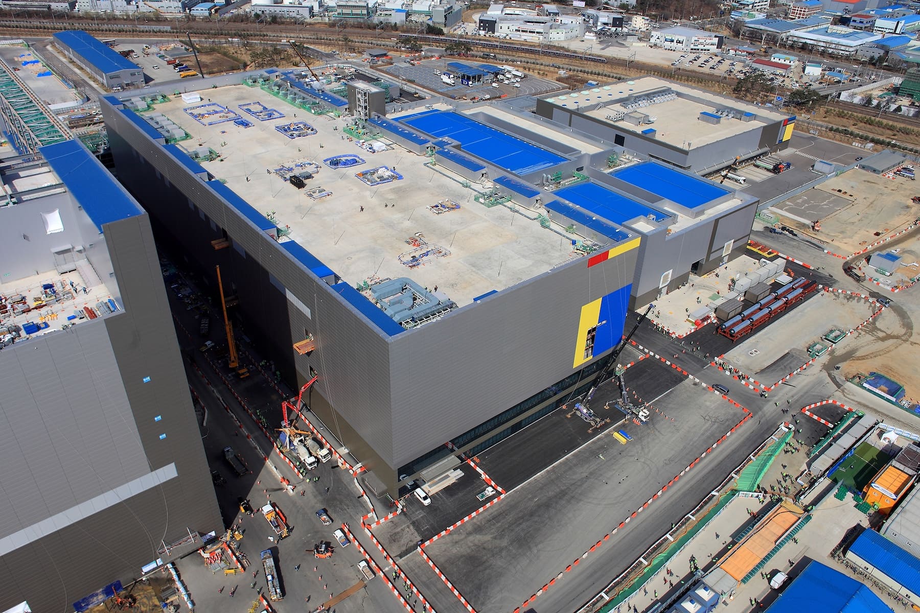
Samsung Electronics’ foundry division begins 2026 with a key indicator that the industry continues to scrutinize: the utilization rate of its factories. According to industry reports published in South Korea, the company anticipates that the average fab utilization will be around 60% during the first half of 2026, up from the 50% range in the second half of 2025. This progress, approximately a 10 percentage point increase, is significant in a business where each percentage point of load can mean the difference between heavy losses and sustained recovery.
Behind this improvement is a very specific factor: more wafers entering production. In other words, more “wafer starts” spread across leading nodes and
The wound of 3 nm and the journey through the drought
Samsung Foundry has faced an uncomfortable narrative in recent years: difficulty securing major clients for advanced processes like 3 nm, a race led by TSMC that has heavily influenced supply decisions across much of the ecosystem. This lack of traction within the premium segment results in a dual problem: less volume on high-end lines and ongoing pressure to sustain investments and cutting-edge equipment without the critical mass of orders to justify the costs.
The result has been a notable decline in profitability for the non-memory chip business. During the worst moments of 2025, the market saw quarterly operating losses in the 2 trillion won range for the non-memory segment, though signs of relief appeared in the second half, bringing the deficit closer to around 1 trillion won thanks to increased activity in key nodes and portfolio adjustments.
2 nm, Exynos, and the “performance” factor: when percentage matters
The increase in utilization isn’t explained solely by traditional demand. Recent months have also seen the start of manufacturing based on 2 nm technology for Samsung’s latest mobile processor, the Exynos 2,600. Estimates from Korea suggest that the yield of this process is around 50% per wafer. While not yet industrial-grade excellence, this level typically marks an important milestone—moving from fine-tuning to more stable production phases.
In foundry, “yield” is the credibility language: it’s not enough to produce; you have to produce well, with a high percentage of usable chips per wafer. As yield improves, the effective cost per chip decreases, boosting competitiveness. More importantly, it builds something that doesn’t appear on financial slides: customer trust.
The big 80% barrier: why 60% isn’t enough
The move to 60% utilization signals recovery but not victory. An industry-documented threshold exists: for a foundry with enormous fixed costs to overcome the “losing money” barrier, it generally needs more than 80% sustained utilization. Industry sources cited in Korea note this level as approximately the break-even point for Samsung Foundry.
The logic is straightforward and brutal. These factories are billion-dollar infrastructures, with high depreciation, significant energy consumption, critical materials, and machinery whose value is justified only if operated at high throughput. At low loads, fixed costs are spread over fewer wafers, eroding margins.
Tesla: the contract that shifted the mood
In this context, any major deal becomes a breathing space. In July 2025, Samsung announced a multiyear chip manufacturing contract for an unidentified client, later publicly linked to Tesla, valued at around $16.5 billion (approximately 22.8 trillion won) to produce the AI6 chip aimed at Artificial Intelligence workloads. Reuters reported that the production would be associated with Samsung’s Taylor (Texas) plant and that Tesla would collaborate to optimize manufacturing efficiency.
Beyond the headline, this deal has several strategic implications: it adds volume, prestige, and a “comeback” narrative at a time when the American plant needed anchor clients to justify its schedule. It also reinforces Samsung’s desire to compete again for high-profile orders—a terrain where every victory is both commercial and symbolic.
The TSMC shadow: overwhelmed demand and a second-mover opportunity
Another factor influencing the debate is capacity tension within the industry. Sources cited by Korean media indicate that TSMC faces supply constraints in advanced processes, creating an opportunity for clients to seek alternatives or diversify risks if this situation persists.
This pressure is also reflected in TSMC’s investment plans. In January 2026, Reuters reported that TSMC plans to raise its capital expenditure in 2026 to between $52 billion and $56 billion, with revenue growth expectations near 30%, fueled by the AI boom. The implicit message is clear: demand not only continues but pushes the industry to expand capacity. When the leader invests heavily, the second-placed player has two options: accept it or accelerate to keep pace.
What to watch for from now on
Reaching 60% utilization is a sign of progress, but the market will demand more:
- Evolution of 2 nm yield and real production stability.
- Samsung’s ability to turn technical advances into repeat customers.
- The pace of replacement and growth in nodes like 4 nm and 8 nm, which remain the main workhorses.
- If the increase in utilization translates into consistent loss reduction and brings the business closer to that 80% threshold deemed critical for profitability.
In an industry accustomed to long cycles and fine-tuned bets, Samsung Foundry is back with a story that’s less about defense and more about rebuilding. The challenge is to turn this rebound into a lasting trend and that trend into sustained profitability.
Frequently Asked Questions
What does it mean that a foundry operates at 60% utilization, and why does it matter?
Utilization indicates how much of the installed capacity is being used. In foundry, 60% suggests growing activity but may still be insufficient to cover very high fixed costs.
Why is more than 80% utilization considered necessary for profitability?
Because machinery and facilities incur massive fixed costs. Beyond a certain load level, the cost per wafer decreases and margins improve significantly.
What is “yield” at 2 nm, and why are clients so concerned?
Yield is the percentage of good chips per wafer. A low yield raises costs and complicates delivery times; a higher yield indicates process maturity and industrial reliability.
How does Tesla’s contract impact Samsung Foundry’s recovery?
It provides volume, visibility, and business credibility, helping justify investments and activity at strategic facilities like Taylor (Texas).
Sources:
- ZDNet Korea (01/19/2026): 60% average utilization forecast for H1, loss contexte, Exynos 2.600 at 2 nm, and an 80% break-even threshold.