Samsung Foundry is once again making moves in the race for advanced semiconductors, but this time with more caution than ambition. According to Korean financial media, the company has once again slowed its schedule for the 1.4-nanometer node and is focusing resources on stabilizing its 2-nanometer process, where a significant portion of its industrial credibility with TSMC is at stake. The underlying message is clear: before promising the next technological frontier, Samsung needs to prove it can truly compete in the current one.
This shift contrasts with the roadmap Samsung presented a few years ago. During its 2022 Foundry Forum and again in 2023, the company scheduled mass production of 1.4 nm for 2027 and the initial deployment of 2 nm for 2025. However, industry reports circulating early 2026 pushed the 1.4 nm timeline to 2029, and now Korean media suggest even that date may not be fixed. At least for now, Samsung has not publicly issued an official statement setting a new definitive schedule for this node.
The priority is no longer to be first, but to get it right
The main reason for this caution is the 2 nm node. Samsung confirmed in its Q4 2025 results that it had already begun mass production of first-generation products fabricated in 2 nm. Its mid-year business report also indicated September 2025 as the start of mass production of the GAA first-generation process aimed at mobile devices. On paper, this means the company is competitive in the race. The problem is that being in the race does not yet mean leading it.
Recent days have seen Korean media suggest that Samsung’s 2 nm process yield has already exceeded 60%, compared to nearly 20% in the second half of 2025. Samsung has not publicly validated this data with detailed figures, so it’s best treated as supply chain information rather than an official number. Still, the improvement aligns with other market signals: higher yields reduce costs, improve wafer utilization, and bring the node closer to a point where it becomes commercially viable for big clients.
This nuance is crucial because Samsung Foundry’s challenges in advanced nodes have not been solely technological but also commercial. TrendForce noted in 2025 that issues stabilizing the 3 nm node contributed to Samsung losing relevant accounts to TSMC, including Apple, NVIDIA, and Google. Additionally, TSMC closed Q4 2025 with a 70.4% share of the global foundry market, while Samsung held just 7.1%. This gap explains why Samsung appears to have adopted a less flashy but arguably more realistic strategy: securing the 2 nm first, then returning to promote the 1.4 nm jump as an imminent promise.
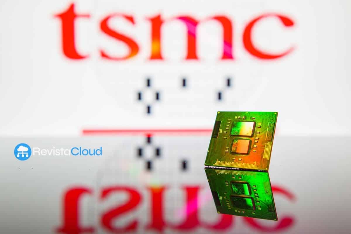
TSMC accelerates while Samsung buys time
The comparison with TSMC helps clarify the pressure. The Taiwanese company officially announced in April 2025 its A14 process, equivalent to a 1.4 nm generation, with scheduled production for 2028. They also stated that their development was ahead of schedule, with yields exceeding expectations. Moreover, TSMC claims its N2 started volume production in Q4 2025, enabling them to offer a highly advanced technology platform that’s difficult for competitors to match today.
This leadership is not just a marketing point. When TSMC lays out a roadmap from N2 to A14 with staggered production and maintains over 70% market share, it signals to major clients a platform with less risk. In contrast, Samsung must convince the market that its 2 nm will be stable, competitive in performance, and mature enough for high-volume designs — especially critical for AI chips, accelerators, premium smartphones, and HPC.
The competitive landscape also includes Rapidus, though in a different position. The Japanese company officially states its pilot line launched in April 2025, with mass production of 2 nm expected in 2027. Asian media also mention its involvement in the 1.4 nm conversation, but the company mainly communicates about its 2 nm roadmap and the progress of its IIM-1 plant in Hokkaido. This means Rapidus is already part of the competitive pressure on Samsung, even if its scale and customer base are still smaller than TSMC’s.
The real battleground is AI chips
All of this is especially crucial for artificial intelligence. The most advanced nodes are increasingly important, not just for mobile processors but also for accelerators, data center ASICs, high-speed networks, and the entire ecosystem surrounding generative AI. Samsung cannot afford to be structurally late to this market, but it also can’t repeat the mistake of having a node announced that fails to perform in practice. Therefore, the apparent delay of 1.4 nm can be seen less as a retreat and more as a strategic prioritization: first, solidify the 2 nm process, then revisit the next leap.
From this perspective, Samsung’s cautious approach makes sense. The company demonstrated in 2022 and 2023 that it aimed to lead with an aggressive roadmap. But four years later, the market is demanding less promise and more execution. If the 2 nm process truly improves in yield, performance, and customer confidence, Samsung will remain the only sizable alternative to TSMC in advanced foundry. If it doesn’t, the delay of the 1.4 nm will be interpreted not as a tactical pause but as evidence that the technological and commercial gap remains open.
Frequently Asked Questions
Has Samsung officially confirmed delaying the 1.4 nm beyond 2029?
Not publicly and in detail. What exists today are a combination of Samsung’s older roadmaps, which pointed to 2027, and more recent industry reports setting the 1.4 nm at 2029 or later.
What does a 2 nm yield around 60% mean?
Simply put, it means a larger proportion of chips fabricated on a wafer are suitable for sale. This is a key indicator for a node to move from experimental to commercially viable and reliable for high-volume customers. For Samsung, this 60% figure is based on reports, not an official company breakdown.
Why does TSMC have an advantage over Samsung in this race?
Because TSMC has officially announced that its N2 entered volume production in Q4 2025, scheduled the A14 node for 2028, and maintains over 70% market share, far ahead of Samsung’s 7.1% at the end of 2025.
Why does this battle over 2 nm and 1.4 nm matter so much for AI?
Because AI chips, accelerators, and high-performance processors rely on advanced nodes to improve density, power consumption, and performance. The first to provide these nodes with solid performance and industrial capacity will have more options to secure the biggest upcoming designs.
via: biz.chosun