The race for high-bandwidth memory (HBM) enters a new phase. Samsung Electronics has set a date and target for its next move: HBM4E with a goal of 3.25 TB/s and mass production in 2027. The company detailed this at the OCP Global Summit 2025 in San Jose, setting a speed per pin of at least 13 Gbps and 2,048 I/O pins to achieve this flow rate, 2.5 times above the current HBM3E. The announcement follows a year in which SK hynix took the lead with HBM3E and positioned itself as the first to commercialize HBM4, while Micron showcased samples at 11 Gbps for its “main AI client”.
The message is clear: Samsung wants to reclaim the throne in memory for AI GPUs and the accelerators leading the industry. And the chosen strategy is speed and efficiency.
From HBM4 to HBM4E: How Did We Get Here?
In January 2025, during ISSCC (San Francisco), Samsung targeted HBM4 at 10 Gbps per pin—a 25% increase over the initial goal of 8 Gbps (2 TB/s) for the JEDEC standard. NVIDIA, the world’s largest buyer of HBM, requested more for its next-generation Vera Rubin accelerators: above 10 Gbps. Samsung responded by raising the speed to 11 Gbps, which SK hynix also adopted. Micron, questioned by analysts about whether they would reach that target, later confirmed 11 Gbps samples to a top-tier client (implicitly, NVIDIA).
With HBM4 already operating above base specifications, industry expectations shifted towards HBM4E climbing another step. Samsung made it official: ≥ 13 Gbps per pin, 3.25 TB/s with 2,048 pins, and double the energy efficiency compared to the current HBM3E at 3.9 pJ/bit. It is the first major manufacturer to openly commit to a “3 TB/s or more” goal for the next generation.
Why It Matters: AI, Bandwidth, and Total Cost of Ownership
The surge of generative AI and LLM training has turned memory bandwidth into the bottleneck. For training, more TB/s means less waiting between GPU and data; for inference, it results in lower latencies and higher throughput per node. Additionally, if energy per bit decreases, the impact on TCO is significant: more performance per watt and lower cost per token at the data center scale.
With HBM4E, Samsung aims for that balance: blazing speed, efficiency, and timelines. Mass production is scheduled for 2027, aligning with the roadmaps for next-gen GPUs.
The Competitive Landscape: SK hynix, Micron… and the “Speed Wars”
- SK hynix has been a benchmark in HBM3E and is positioning itself as first with HBM4. Samsung’s announcement aims to press the pace with HBM4E and 3.25 TB/s, a way to get ahead on the next curve.
- Micron mitigated doubts by confirming samples of 11 Gbps with HBM4. The challenge for the trio will be sustaining performance and capacity as NVIDIA and other hyperscalers ramp up orders.
The rise of AI demand has upended traditional memory cycle logic. Beyond DDR5/DDR4, capital expenditure and engineering talent are focused on HBM—where the margin lies. Therefore, every specification announcement also acts as a market signal: who is leading, who is following, and who will arrive on time for the next GPU integration window.
What Samsung Has Said: HBM4E, LPDDR6, and 2 nm Foundry
The South Korean manufacturer used the OCP Global Summit 2025 to paint a comprehensive picture:
- HBM4E: ≥ 13 Gbps per pin, 2,048 pins, 3.25 TB/s, and > 2× energy efficiency improvement over HBM3E. Mass production slated for 2027.
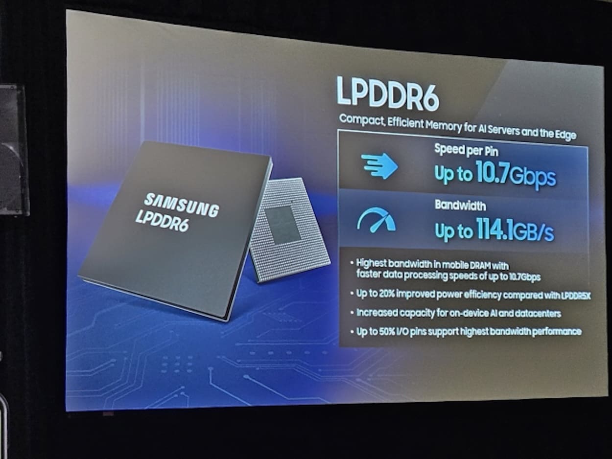
- LPDDR6: first product with 10.7 Gbps per pin and 114.1 GB/s bandwidth, 20% more efficient than LPDDR5X. This mobile memory will power SoCs and devices also scaling AI at the edge.
- 2 nm (SF2) fabrication: ready and with production expected by late 2025. In parallel, collaboration with Rebellions for their Rebel Quad, which will incorporate an ARM Neoverse V3 CPU (“Rebel-CPU”) and an NPU manufactured using SF2 (2 nm) and SF4X (4 nm). CPU clock targets are between 3.5–4.0 GHz, above the 3.44 GHz of Grace CPU (Neoverse V2, 4 nm from TSMC).
Beyond the HBM metric, Samsung emphasizes that its entire supply chain—memory, mobile DRAM, and foundry nodes—aligns with the upcoming wave of AI-centric products.
What Does 3.25 TB/s Mean… and What Still Needs To Be Answered?
3.25 TB/s is the sum of 13 Gbps per pin × 2,048 pins × (1 byte/8 bits). It’s not just a round number: it encompasses interfaces,
What remains unknown?
- Effective latencies and energy per bit in real silicon. Samsung talks about >2× improvement over HBM3E (3.9 pJ/bit), but consumption curves at various frequencies are still missing.
- Capacities per stack and densities, crucial for LLM training, where the fit of the model within each GPU makes a difference.
- Availability coordinated with GPU. A HBM4E ready in 2027 will need anchor customers—e.g., NVIDIA, AMD, others—with drivers and back-end support prepared.
Why Efficiency Is Just as Important as Speed
Achieving 3.25 TB/s requires ≥ 13 Gbps per pin. Each speed increment heightens signal and power challenges. That’s why the promise of energy per bit being >2× better than HBM3E is so significant: lower than 3.9 pJ/bit means less heat and higher density per rack before hitting thermal limits. In a market where power consumption and cooling increase costs, pJ/bit becomes a KPI as vital as Gbps.
Changing the Throne? The Cards Being Played Toward 2027
Leadership in HBM isn’t just about “who’s first”; it’s about who can deliver volume with sustained performance, high manufacturing yields, and consistent quality. SK hynix is ahead with HBM3E and their plan for HBM4. Micron has demonstrated strength with samples at 11 Gbps. Samsung is positioning itself with HBM4E and 3.25 TB/s as a strategic move to reshape the landscape. The market will determine whether that bandwidth target translates into contracts and capacity in time for the GPUs of the later half of the decade.
And the Rest of the Portfolio? LPDDR6 and 2 nm Also Play
The announcement of LPDDR6 (10.7 Gbps, 114.1 GB/s, +20% efficiency vs. LPDDR5X) aligns with the AI decentralization: mobile devices, PCs with NPUs, and edge computing. Moving to 2 nm (SF2) also brings Samsung closer to the elite seeking frequencies and efficiency for the next wave. The partnership with Rebellions—a South Korean AI chip startup—also serves as a showcase of what’s possible when combining CPU + NPU using SF2 and SF4X.